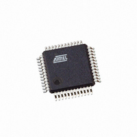
ATMEGA406-1AAU Atmel, ATMEGA406-1AAU Datasheet - Page 150

ATMEGA406-1AAU
Manufacturer Part Number
ATMEGA406-1AAU
Description
IC AVR MCU 40K 1MHZ 48LQFP
Manufacturer
Atmel
Series
AVR® ATmegar
Specifications of ATMEGA406-1AAU
Core Processor
AVR
Core Size
8-Bit
Speed
1MHz
Connectivity
I²C
Peripherals
POR, WDT
Number Of I /o
18
Program Memory Size
40KB (20K x 16)
Program Memory Type
FLASH
Eeprom Size
512 x 8
Ram Size
2K x 8
Voltage - Supply (vcc/vdd)
4 V ~ 25 V
Data Converters
A/D 10x12b
Oscillator Type
Internal
Operating Temperature
-30°C ~ 85°C
Package / Case
48-LQFP
Processor Series
ATMEGA48x
Core
AVR8
Data Bus Width
8 bit
Data Ram Size
2 KB
Interface Type
2-Wire
Maximum Clock Frequency
1 MHz
Number Of Programmable I/os
18
Number Of Timers
2
Maximum Operating Temperature
+ 85 C
Mounting Style
SMD/SMT
3rd Party Development Tools
EWAVR, EWAVR-BL
Development Tools By Supplier
ATAVRDRAGON, ATSTK500, ATSTK600, ATAVRISP2, ATAVRONEKIT
Minimum Operating Temperature
- 30 C
Cpu Family
ATmega
Device Core
AVR
Device Core Size
8b
Frequency (max)
1MHz
Total Internal Ram Size
2KB
# I/os (max)
18
Number Of Timers - General Purpose
2
Operating Supply Voltage (typ)
5/9/12/15/18/24V
Operating Supply Voltage (max)
25V
Operating Supply Voltage (min)
4V
On-chip Adc
10-chx12-bit
Instruction Set Architecture
RISC
Operating Temp Range
-30C to 85C
Operating Temperature Classification
Commercial
Mounting
Surface Mount
Pin Count
48
Package Type
LQFP
Controller Family/series
AVR MEGA
No. Of I/o's
18
Eeprom Memory Size
512Byte
Ram Memory Size
2KB
Cpu Speed
1MHz
Rohs Compliant
Yes
For Use With
770-1007 - ISP 4PORT ATMEL AVR MCU SPI/JTAG770-1005 - ISP 4PORT FOR ATMEL AVR MCU JTAG770-1004 - ISP 4PORT FOR ATMEL AVR MCU SPI
Lead Free Status / RoHS Status
Lead free / RoHS Compliant
Available stocks
Company
Part Number
Manufacturer
Quantity
Price
Part Number:
ATMEGA406-1AAU
Manufacturer:
AT
Quantity:
20 000
25.6.6
25.7
150
Using the TWI
ATmega406
TWAMR – TWI (Slave) Address Mask Register
• Bit 0 – TWGCE: TWI General Call Recognition Enable Bit
If set, this bit enables the recognition of a General Call given over the Two-wire Serial Bus.
• Bits 7:1 – TWAM: TWI Address Mask
The TWAMR can be loaded with a 7-bit Slave Address mask. Each of the bits in TWAMR can
mask (disable) the corresponding address bits in the TWI Address Register (TWAR). If the mask
bit is set to one then the address match logic ignores the compare between the incoming
address bit and the corresponding bit in TWAR.
detail.
Figure 25-10. TWI Address Match Logic, Block Diagram
• Bit 0 – Res: Reserved Bit
This bit is an unused bit in the ATmega406, and will always read as zero.
The AVR TWI is byte-oriented and interrupt based. Interrupts are issued after all bus events, like
reception of a byte or transmission of a START condition. Because the TWI is interrupt-based,
the application software is free to carry on other operations during a TWI byte transfer. Note that
the TWI Interrupt Enable (TWIE) bit in TWCR together with the Global Interrupt Enable bit in
SREG allow the application to decide whether or not assertion of the TWINT flag should gener-
ate an interrupt request. If the TWIE bit is cleared, the application must poll the TWINT flag in
order to detect actions on the TWI bus.
When the TWINT flag is asserted, the TWI has finished an operation and awaits application
response. In this case, the TWI Status Register (TWSR) contains a value indicating the current
state of the TWI bus. The application software can then decide how the TWI should behave in
the next TWI bus cycle by manipulating the TWCR and TWDR registers.
Figure 25-11
this example, a Master wishes to transmit a single data byte to a Slave. This description is quite
abstract, a more detailed explanation follows later in this section. A simple code example imple-
menting the desired behavior is also presented.
Bit
(0xBD)
Read/Write
Initial Value
TWAMR0
Address
TWAR0
Bit 0
is a simple example of how the application can interface to the TWI hardware. In
R/W
7
0
R/W
6
0
Address Bit Comparator 6..1
R/W
5
0
Address Bit Comparator 0
TWAM[6:0]
R/W
4
0
Figure 25-10
R/W
3
0
R/W
shown the address match logic in
2
0
R/W
1
0
Address
R
Match
0
–
0
2548E–AVR–07/06
TWAMR


