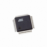
ATMEGA406-1AAU Atmel, ATMEGA406-1AAU Datasheet - Page 171

ATMEGA406-1AAU
Manufacturer Part Number
ATMEGA406-1AAU
Description
IC AVR MCU 40K 1MHZ 48LQFP
Manufacturer
Atmel
Series
AVR® ATmegar
Specifications of ATMEGA406-1AAU
Core Processor
AVR
Core Size
8-Bit
Speed
1MHz
Connectivity
I²C
Peripherals
POR, WDT
Number Of I /o
18
Program Memory Size
40KB (20K x 16)
Program Memory Type
FLASH
Eeprom Size
512 x 8
Ram Size
2K x 8
Voltage - Supply (vcc/vdd)
4 V ~ 25 V
Data Converters
A/D 10x12b
Oscillator Type
Internal
Operating Temperature
-30°C ~ 85°C
Package / Case
48-LQFP
Processor Series
ATMEGA48x
Core
AVR8
Data Bus Width
8 bit
Data Ram Size
2 KB
Interface Type
2-Wire
Maximum Clock Frequency
1 MHz
Number Of Programmable I/os
18
Number Of Timers
2
Maximum Operating Temperature
+ 85 C
Mounting Style
SMD/SMT
3rd Party Development Tools
EWAVR, EWAVR-BL
Development Tools By Supplier
ATAVRDRAGON, ATSTK500, ATSTK600, ATAVRISP2, ATAVRONEKIT
Minimum Operating Temperature
- 30 C
Cpu Family
ATmega
Device Core
AVR
Device Core Size
8b
Frequency (max)
1MHz
Total Internal Ram Size
2KB
# I/os (max)
18
Number Of Timers - General Purpose
2
Operating Supply Voltage (typ)
5/9/12/15/18/24V
Operating Supply Voltage (max)
25V
Operating Supply Voltage (min)
4V
On-chip Adc
10-chx12-bit
Instruction Set Architecture
RISC
Operating Temp Range
-30C to 85C
Operating Temperature Classification
Commercial
Mounting
Surface Mount
Pin Count
48
Package Type
LQFP
Controller Family/series
AVR MEGA
No. Of I/o's
18
Eeprom Memory Size
512Byte
Ram Memory Size
2KB
Cpu Speed
1MHz
Rohs Compliant
Yes
For Use With
770-1007 - ISP 4PORT ATMEL AVR MCU SPI/JTAG770-1005 - ISP 4PORT FOR ATMEL AVR MCU JTAG770-1004 - ISP 4PORT FOR ATMEL AVR MCU SPI
Lead Free Status / RoHS Status
Lead free / RoHS Compliant
Available stocks
Company
Part Number
Manufacturer
Quantity
Price
Part Number:
ATMEGA406-1AAU
Manufacturer:
AT
Quantity:
20 000
26. JTAG Interface and On-chip Debug System
26.1
26.2
26.3
2548E–AVR–07/06
Features
Overview
Test Access Port – TAP
•
•
•
•
•
The AVR IEEE std. 1149.1 compliant JTAG interface can be used for
• Programming the non-volatile memories, Fuses and Lock bits
• On-chip debugging
A brief description is given in the following sections. Detailed descriptions for Programming via
the JTAG interface can be found in the section
211. The On-chip Debug support is considered being private JTAG instructions, and distributed
within ATMEL and to selected third party vendors only.
Figure 26-1
TAP Controller is a state machine controlled by the TCK and TMS signals. The TAP Controller
selects either the JTAG Instruction Register or one of several Data Registers as the scan chain
(Shift Register) between the TDI – input and TDO – output. The Instruction Register holds JTAG
instructions controlling the behavior of a Data Register.
The JTAG Programming Interface (actually consisting of several physical and virtual Data Reg-
isters) is used for serial programming via the JTAG interface. The Internal Scan Chain and
Break Point Scan Chain are used for On-chip debugging only.
The JTAG interface is accessed through four of the AVR’s pins. In JTAG terminology, these pins
constitute the Test Access Port – TAP. These pins are:
• TMS: Test mode select. This pin is used for navigating through the TAP-controller state
• TCK: Test Clock. JTAG operation is synchronous to TCK.
• TDI: Test Data In. Serial input data to be shifted in to the Instruction Register or Data Register
• TDO: Test Data Out. Serial output data from Instruction Register or Data Register.
machine.
(Scan Chains).
JTAG (IEEE std. 1149.1 Compliant) Interface
Debugger Access to:
Extensive On-chip Debug Support for Break Conditions, Including
Programming of Flash, EEPROM, Fuses, and Lock Bits through the JTAG Interface
On-chip Debugging Supported by AVR Studio
– All Internal Peripheral Units
– Internal and External RAM
– The Internal Register File
– Program Counter
– EEPROM and Flash Memories
– AVR Break Instruction
– Break on Change of Program Memory Flow
– Single Step Break
– Program Memory Break Points on Single Address or Address Range
– Data Memory Break Points on Single Address or Address Range
shows a block diagram of the JTAG interface and the On-chip Debug system. The
®
”Programming via the JTAG Interface” on page
ATmega406
171


