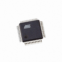
ATMEGA406-1AAU Atmel, ATMEGA406-1AAU Datasheet - Page 145

ATMEGA406-1AAU
Manufacturer Part Number
ATMEGA406-1AAU
Description
IC AVR MCU 40K 1MHZ 48LQFP
Manufacturer
Atmel
Series
AVR® ATmegar
Specifications of ATMEGA406-1AAU
Core Processor
AVR
Core Size
8-Bit
Speed
1MHz
Connectivity
I²C
Peripherals
POR, WDT
Number Of I /o
18
Program Memory Size
40KB (20K x 16)
Program Memory Type
FLASH
Eeprom Size
512 x 8
Ram Size
2K x 8
Voltage - Supply (vcc/vdd)
4 V ~ 25 V
Data Converters
A/D 10x12b
Oscillator Type
Internal
Operating Temperature
-30°C ~ 85°C
Package / Case
48-LQFP
Processor Series
ATMEGA48x
Core
AVR8
Data Bus Width
8 bit
Data Ram Size
2 KB
Interface Type
2-Wire
Maximum Clock Frequency
1 MHz
Number Of Programmable I/os
18
Number Of Timers
2
Maximum Operating Temperature
+ 85 C
Mounting Style
SMD/SMT
3rd Party Development Tools
EWAVR, EWAVR-BL
Development Tools By Supplier
ATAVRDRAGON, ATSTK500, ATSTK600, ATAVRISP2, ATAVRONEKIT
Minimum Operating Temperature
- 30 C
Cpu Family
ATmega
Device Core
AVR
Device Core Size
8b
Frequency (max)
1MHz
Total Internal Ram Size
2KB
# I/os (max)
18
Number Of Timers - General Purpose
2
Operating Supply Voltage (typ)
5/9/12/15/18/24V
Operating Supply Voltage (max)
25V
Operating Supply Voltage (min)
4V
On-chip Adc
10-chx12-bit
Instruction Set Architecture
RISC
Operating Temp Range
-30C to 85C
Operating Temperature Classification
Commercial
Mounting
Surface Mount
Pin Count
48
Package Type
LQFP
Controller Family/series
AVR MEGA
No. Of I/o's
18
Eeprom Memory Size
512Byte
Ram Memory Size
2KB
Cpu Speed
1MHz
Rohs Compliant
Yes
For Use With
770-1007 - ISP 4PORT ATMEL AVR MCU SPI/JTAG770-1005 - ISP 4PORT FOR ATMEL AVR MCU JTAG770-1004 - ISP 4PORT FOR ATMEL AVR MCU SPI
Lead Free Status / RoHS Status
Lead free / RoHS Compliant
Available stocks
Company
Part Number
Manufacturer
Quantity
Price
Part Number:
ATMEGA406-1AAU
Manufacturer:
AT
Quantity:
20 000
25.5.2
25.5.3
25.5.4
2548E–AVR–07/06
Bit Rate Generator Unit
Bus Interface Unit
Address Match Unit
This unit controls the period of SCL when operating in a Master mode. The SCL period is con-
trolled by settings in the TWI Bit Rate Register (TWBR) and the Prescaler bits in the TWI Status
Register (TWSR). Slave operation does not depend on Bit Rate or Prescaler settings, but the
CPU clock frequency in the slave must be at least 16 times higher than the SCL frequency. Note
that slaves may prolong the SCL low period, thereby reducing the average TWI bus clock
period. The SCL frequency is generated according to the following equation:
• TWBR = Value of the TWI Bit Rate Register.
• TWPS = Value of the prescaler bits in the TWI Status Register.
Notes:
This unit contains the Data and Address Shift Register (TWDR), a START/STOP Controller and
Arbitration detection hardware. The TWDR contains the address or data bytes to be transmitted,
or the address or data bytes received. In addition to the 8-bit TWDR, the Bus Interface Unit also
contains a register containing the (N)ACK bit to be transmitted or received. This (N)ACK Regis-
ter is not directly accessible by the application software. However, when receiving, it can be set
or cleared by manipulating the TWI Control Register (TWCR). When in Transmitter mode, the
value of the received (N)ACK bit can be determined by the value in the TWSR.
The START/STOP Controller is responsible for generation and detection of START, REPEATED
START, and STOP conditions. The START/STOP controller is able to detect START and STOP
conditions even when the AVR MCU is in one of the sleep modes, enabling the MCU to wake up
if addressed by a Master.
If the TWI has initiated a transmission as Master, the Arbitration Detection hardware continu-
ously monitors the transmission trying to determine if arbitration is in process. If the TWI has lost
an arbitration, the Control Unit is informed. Correct action can then be taken and appropriate
status codes generated.
The Address Match unit checks if received address bytes match the 7-bit address in the TWI
Address Register (TWAR). If the TWI General Call Recognition Enable (TWGCE) bit in the
TWAR is written to one, all incoming address bits will also be compared against the General Call
address. Upon an address match, the Control unit is informed, allowing correct action to be
taken. The TWI may or may not acknowledge its address, depending on settings in the TWCR.
The Address Match unit is able to compare addresses even when the AVR MCU is in sleep
mode, enabling the MCU to wake-up if addressed by a Master.
1. TWBR should be 10 or higher if the TWI operates in Master mode. If TWBR is lower than 10,
2. The TWI clock is 4 MHz, see “Calibrated Fast RC Oscillator” on page 26.
the master may produce an incorrect output on SDA and SCL for the reminder of the byte. The
problem occurs when operating the TWI in Master mode, sending Start + SLA + R/W to a
slave (a slave does not need to be connected to the bus for the condition to happen).
SCL frequency
=
---------------------------------------------------------- -
16
TWI Clock frequency
+
2(TWBR) 4
⋅
TWPS
ATmega406
145


