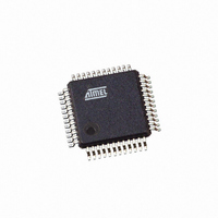
ATMEGA406-1AAU Atmel, ATMEGA406-1AAU Datasheet - Page 60

ATMEGA406-1AAU
Manufacturer Part Number
ATMEGA406-1AAU
Description
IC AVR MCU 40K 1MHZ 48LQFP
Manufacturer
Atmel
Series
AVR® ATmegar
Specifications of ATMEGA406-1AAU
Core Processor
AVR
Core Size
8-Bit
Speed
1MHz
Connectivity
I²C
Peripherals
POR, WDT
Number Of I /o
18
Program Memory Size
40KB (20K x 16)
Program Memory Type
FLASH
Eeprom Size
512 x 8
Ram Size
2K x 8
Voltage - Supply (vcc/vdd)
4 V ~ 25 V
Data Converters
A/D 10x12b
Oscillator Type
Internal
Operating Temperature
-30°C ~ 85°C
Package / Case
48-LQFP
Processor Series
ATMEGA48x
Core
AVR8
Data Bus Width
8 bit
Data Ram Size
2 KB
Interface Type
2-Wire
Maximum Clock Frequency
1 MHz
Number Of Programmable I/os
18
Number Of Timers
2
Maximum Operating Temperature
+ 85 C
Mounting Style
SMD/SMT
3rd Party Development Tools
EWAVR, EWAVR-BL
Development Tools By Supplier
ATAVRDRAGON, ATSTK500, ATSTK600, ATAVRISP2, ATAVRONEKIT
Minimum Operating Temperature
- 30 C
Cpu Family
ATmega
Device Core
AVR
Device Core Size
8b
Frequency (max)
1MHz
Total Internal Ram Size
2KB
# I/os (max)
18
Number Of Timers - General Purpose
2
Operating Supply Voltage (typ)
5/9/12/15/18/24V
Operating Supply Voltage (max)
25V
Operating Supply Voltage (min)
4V
On-chip Adc
10-chx12-bit
Instruction Set Architecture
RISC
Operating Temp Range
-30C to 85C
Operating Temperature Classification
Commercial
Mounting
Surface Mount
Pin Count
48
Package Type
LQFP
Controller Family/series
AVR MEGA
No. Of I/o's
18
Eeprom Memory Size
512Byte
Ram Memory Size
2KB
Cpu Speed
1MHz
Rohs Compliant
Yes
For Use With
770-1007 - ISP 4PORT ATMEL AVR MCU SPI/JTAG770-1005 - ISP 4PORT FOR ATMEL AVR MCU JTAG770-1004 - ISP 4PORT FOR ATMEL AVR MCU SPI
Lead Free Status / RoHS Status
Lead free / RoHS Compliant
Available stocks
Company
Part Number
Manufacturer
Quantity
Price
Part Number:
ATMEGA406-1AAU
Manufacturer:
AT
Quantity:
20 000
13. Low Voltage I/O-Ports
13.1
60
Introduction
ATmega406
All low voltage AVR ports have true Read-Modify-Write functionality when used as general digi-
tal I/O ports. This means that the direction of one port pin can be changed without unintentionally
changing the direction of any other pin with the SBI and CBI instructions. The same applies
when changing drive value (if configured as output) or enabling/disabling of pull-up resistors (if
configured as input). All low voltage port pins have individually selectable pull-up resistors with a
supply-voltage invariant resistance. All I/O pins have protection diodes to both V
as indicated in
complete list of parameters.
Figure 13-1. Low Voltage I/O Pin Equivalent Schematic
All registers and bit references in this section are written in general form. A lower case “x” repre-
sents the numbering letter for the port, and a lower case “n” represents the bit number. However,
when using the register or bit defines in a program, the precise form must be used. For example,
PORTB3 for bit no. 3 in Port B, here documented generally as PORTxn. The physical I/O Regis-
ters and bit locations are listed in
Three I/O memory address locations are allocated for each low voltage port, one each for the
Data Register – PORTx, Data Direction Register – DDRx, and the Port Input Pins – PINx. The
Port Input Pins I/O location is read only, while the Data Register and the Data Direction Register
are read/write. However, writing a logic one to a bit in the PINx Register, will result in a toggle in
the corresponding bit in the Data Register. In addition, the Pull-up Disable – PUD bit in MCUCR
disables the pull-up function for all low voltage pins in all ports when set.
Using the I/O port as General Digital I/O is described in
I/O” on page
peripheral features on the device. How each alternate function interferes with the port pin is
described in
full description of the alternate functions.
Note that enabling the alternate function of some of the port pins does not affect the use of the
other pins in the port as general digital I/O.
”Alternate Port Functions” on page
61. Many low voltage port pins are multiplexed with alternate functions for the
Pxn
Figure 13-1 on page
”Register Description” on page
C
pin
60. Refer to
66. Refer to the individual module sections for a
”Electrical Characteristics” on page 225
”Low Voltage Ports as General Digital
"General Digital I/O" for
73.
See Figure
R
Details
pu
Logic
REG
2548E–AVR–07/06
and Ground
for a


