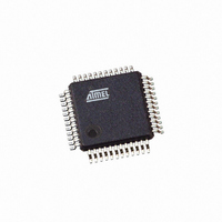
ATMEGA406-1AAU Atmel, ATMEGA406-1AAU Datasheet - Page 183

ATMEGA406-1AAU
Manufacturer Part Number
ATMEGA406-1AAU
Description
IC AVR MCU 40K 1MHZ 48LQFP
Manufacturer
Atmel
Series
AVR® ATmegar
Specifications of ATMEGA406-1AAU
Core Processor
AVR
Core Size
8-Bit
Speed
1MHz
Connectivity
I²C
Peripherals
POR, WDT
Number Of I /o
18
Program Memory Size
40KB (20K x 16)
Program Memory Type
FLASH
Eeprom Size
512 x 8
Ram Size
2K x 8
Voltage - Supply (vcc/vdd)
4 V ~ 25 V
Data Converters
A/D 10x12b
Oscillator Type
Internal
Operating Temperature
-30°C ~ 85°C
Package / Case
48-LQFP
Processor Series
ATMEGA48x
Core
AVR8
Data Bus Width
8 bit
Data Ram Size
2 KB
Interface Type
2-Wire
Maximum Clock Frequency
1 MHz
Number Of Programmable I/os
18
Number Of Timers
2
Maximum Operating Temperature
+ 85 C
Mounting Style
SMD/SMT
3rd Party Development Tools
EWAVR, EWAVR-BL
Development Tools By Supplier
ATAVRDRAGON, ATSTK500, ATSTK600, ATAVRISP2, ATAVRONEKIT
Minimum Operating Temperature
- 30 C
Cpu Family
ATmega
Device Core
AVR
Device Core Size
8b
Frequency (max)
1MHz
Total Internal Ram Size
2KB
# I/os (max)
18
Number Of Timers - General Purpose
2
Operating Supply Voltage (typ)
5/9/12/15/18/24V
Operating Supply Voltage (max)
25V
Operating Supply Voltage (min)
4V
On-chip Adc
10-chx12-bit
Instruction Set Architecture
RISC
Operating Temp Range
-30C to 85C
Operating Temperature Classification
Commercial
Mounting
Surface Mount
Pin Count
48
Package Type
LQFP
Controller Family/series
AVR MEGA
No. Of I/o's
18
Eeprom Memory Size
512Byte
Ram Memory Size
2KB
Cpu Speed
1MHz
Rohs Compliant
Yes
For Use With
770-1007 - ISP 4PORT ATMEL AVR MCU SPI/JTAG770-1005 - ISP 4PORT FOR ATMEL AVR MCU JTAG770-1004 - ISP 4PORT FOR ATMEL AVR MCU SPI
Lead Free Status / RoHS Status
Lead free / RoHS Compliant
Available stocks
Company
Part Number
Manufacturer
Quantity
Price
Part Number:
ATMEGA406-1AAU
Manufacturer:
AT
Quantity:
20 000
27.5
27.5.1
2548E–AVR–07/06
Entering the Boot Loader Program
SPMCSR – Store Program Memory Control and Status Register
Entering the Boot Loader takes place by a jump or call from the application program. This may
be initiated by a trigger such as a command received via the TWI interface. Alternatively, the
Boot Reset Fuse can be programmed so that the Reset Vector is pointing to the Boot Flash start
address after a reset. In this case, the Boot Loader is started after a reset. After the application
code is loaded, the program can start executing the application code. Note that the fuses cannot
be changed by the MCU itself. This means that once the Boot Reset Fuse is programmed, the
Reset Vector will always point to the Boot Loader Reset and the fuse can only be changed
through the serial or parallel programming interface.
Table 27-4.
Note:
The Store Program Memory Control and Status Register contains the control bits needed to con-
trol the Boot Loader operations.
• Bit 7 – SPMIE: SPM Interrupt Enable
When the SPMIE bit is written to one, and the I-bit in the Status Register is set (one), the SPM
ready interrupt will be enabled. The SPM ready Interrupt will be executed as long as the SPMEN
bit in the SPMCSR Register is cleared.
• Bit 6 – RWWSB: Read-While-Write Section Busy
When a Self-Programming (Page Erase or Page Write) operation to the RWW section is initi-
ated, the RWWSB will be set (one) by hardware. When the RWWSB bit is set, the RWW section
cannot be accessed. The RWWSB bit will be cleared if the RWWSRE bit is written to one after a
Self-Programming operation is completed. Alternatively the RWWSB bit will automatically be
cleared if a page load operation is initiated.
• Bit 5 - SIGRD: Signature Row Read
If this bit is written to one at the same time as SPMEN, the next LPM instruction within three
clock cycles will read a byte from the signature row into the destination register. see “Reading
the Signature Row from Software” on page 189 for details.
An SPM instruction within four cycles after SIGRD and SPMEN are set will have no effect. This
operation is reserved for future use and should not be used.
Bit
0x37 (0x57)
Read/Write
Initial Value
BOOTRST
1
0
1. “1” means unprogrammed, “0” means programmed
SPMIE
Boot Reset Fuse
R/W
7
0
Reset Address
Reset Vector = Application Reset (address 0x0000)
Reset Vector = Boot Loader Reset (see
RWWSB
R
6
0
(1)
SIGRD
R/W
5
0
RWWSRE
R/W
4
0
BLBSET
R/W
3
0
Table 27-7 on page
PGWRT
R/W
2
0
PGERS
R/W
1
0
193)
ATmega406
SPMEN
R/W
0
0
SPMCSR
183


