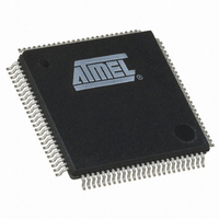
AT91SAM7A3-AU Atmel, AT91SAM7A3-AU Datasheet - Page 116

AT91SAM7A3-AU
Manufacturer Part Number
AT91SAM7A3-AU
Description
IC ARM7 MCU FLASH 256K 100LQFP
Manufacturer
Atmel
Series
AT91SAMr
Specifications of AT91SAM7A3-AU
Core Processor
ARM7
Core Size
16/32-Bit
Speed
60MHz
Connectivity
CAN, I²C, MMC, SPI, SSC, UART/USART
Peripherals
POR, PWM, WDT
Number Of I /o
62
Program Memory Size
256KB (256K x 8)
Program Memory Type
FLASH
Ram Size
32K x 8
Voltage - Supply (vcc/vdd)
1.65 V ~ 1.95 V
Data Converters
A/D 8x10b
Oscillator Type
Internal
Operating Temperature
-40°C ~ 85°C
Package / Case
100-LQFP
Controller Family/series
AT91SAM7xx
No. Of I/o's
62
Ram Memory Size
32KB
Cpu Speed
60MHz
No. Of Timers
3
Rohs Compliant
Yes
Package
100LQFP
Device Core
ARM7TDMI
Family Name
91S
Maximum Speed
60 MHz
Operating Supply Voltage
3.3 V
Data Bus Width
32 Bit
Number Of Programmable I/os
62
Interface Type
CAN/SPI/I2S/TWI/USART/USB
On-chip Adc
2(8-chx10-bit)
Number Of Timers
3
Processor Series
AT91SAMx
Core
ARM7TDMI
Data Ram Size
32 KB
Maximum Clock Frequency
60 MHz
Maximum Operating Temperature
+ 85 C
Mounting Style
SMD/SMT
3rd Party Development Tools
JTRACE-ARM-2M, MDK-ARM, RL-ARM, ULINK2
Development Tools By Supplier
AT91SAM-ICE, AT91-ISP, AT91SAM7A3-EK
Minimum Operating Temperature
- 40 C
Cpu Family
91S
Device Core Size
32b
Frequency (max)
60MHz
Total Internal Ram Size
32KB
# I/os (max)
62
Number Of Timers - General Purpose
3
Operating Supply Voltage (typ)
3.3V
Operating Supply Voltage (max)
3.6V
Operating Supply Voltage (min)
3V
Instruction Set Architecture
RISC
Operating Temp Range
-40C to 85C
Operating Temperature Classification
Industrial
Mounting
Surface Mount
Pin Count
100
Package Type
LQFP
For Use With
AT91SAM-ICE - EMULATOR FOR AT91 ARM7/ARM9AT91SAM7A3-EK - KIT EVAL FOR AT91SAM7A3
Lead Free Status / RoHS Status
Lead free / RoHS Compliant
Eeprom Size
-
Lead Free Status / Rohs Status
Details
Available stocks
Company
Part Number
Manufacturer
Quantity
Price
Company:
Part Number:
AT91SAM7A3-AU
Manufacturer:
MXIC
Quantity:
1 001
Company:
Part Number:
AT91SAM7A3-AU
Manufacturer:
Atmel
Quantity:
730
- Current page: 116 of 594
- Download datasheet (7Mb)
21.3
21.3.1
21.3.2
21.3.3
116
Functional Description
AT91SAM7A3 Preliminary
Configuration
Memory Pointers
Transfer Counters
The PDC channels user interface enables the user to configure and control the data transfers
for each channel. The user interface of a PDC channel is integrated into the user interface of
the peripheral (offset 0x100), which it is related to.
Per peripheral, it contains four 32-bit Pointer Registers (RPR, RNPR, TPR, and TNPR) and
four 16-bit Counter Registers (RCR, RNCR, TCR, and TNCR).
The size of the buffer (number of transfers) is configured in an internal 16-bit transfer counter
register, and it is possible, at any moment, to read the number of transfers left for each
channel.
The memory base address is configured in a 32-bit memory pointer by defining the location of
the first address to access in the memory. It is possible, at any moment, to read the location in
memory of the next transfer and the number of remaining transfers. The PDC has dedicated
status registers which indicate if the transfer is enabled or disabled for each channel. The sta-
tus for each channel is located in the peripheral status register. Transfers can be enabled
and/or disabled by setting TXTEN/TXTDIS and RXTEN/RXTDIS in PDC Transfer Control
Register. These control bits enable reading the pointer and counter registers safely without
any risk of their changing between both reads.
The PDC sends status flags to the peripheral visible in its status-register (ENDRX, ENDTX,
RXBUFF, and TXBUFE).
ENDRX flag is set when the PERIPH_RCR register reaches zero.
RXBUFF flag is set when both PERIPH_RCR and PERIPH_RNCR reach zero.
ENDTX flag is set when the PERIPH_TCR register reaches zero.
TXBUFE flag is set when both PERIPH_TCR and PERIPH_TNCR reach zero.
These status flags are described in the peripheral status register.
Each peripheral is connected to the PDC by a receiver data channel and a transmitter data
channel. Each channel has an internal 32-bit memory pointer. Each memory pointer points to
a location anywhere in the memory space (on-chip memory or external bus interface memory).
Depending on the type of transfer (byte, half-word or word), the memory pointer is incre-
mented by 1, 2 or 4, respectively for peripheral transfers.
If a memory pointer is reprogrammed while the PDC is in operation, the transfer address is
changed, and the PDC performs transfers using the new address.
There is one internal 16-bit transfer counter for each channel used to count the size of the
block already transferred by its associated channel. These counters are decremented after
each data transfer. When the counter reaches zero, the transfer is complete and the PDC
stops transferring data.
If the Next Counter Register is equal to zero, the PDC disables the trigger while activating the
related peripheral end flag.
6042E–ATARM–14-Dec-06
Related parts for AT91SAM7A3-AU
Image
Part Number
Description
Manufacturer
Datasheet
Request
R

Part Number:
Description:
MCU ARM9 64K SRAM 144-LFBGA
Manufacturer:
Atmel
Datasheet:

Part Number:
Description:
IC ARM9 MPU 217-LFBGA
Manufacturer:
Atmel
Datasheet:

Part Number:
Description:
MCU ARM9 ULTRA LOW PWR 217-LFBGA
Manufacturer:
Atmel
Datasheet:

Part Number:
Description:
MCU ARM9 324-TFBGA
Manufacturer:
Atmel
Datasheet:

Part Number:
Description:
IC MCU ARM9 SAMPLING 217CBGA
Manufacturer:
Atmel
Datasheet:

Part Number:
Description:
IC ARM9 MCU 217-LFBGA
Manufacturer:
Atmel
Datasheet:

Part Number:
Description:
IC ARM9 MCU 208-PQFP
Manufacturer:
Atmel
Datasheet:

Part Number:
Description:
MCU ARM 512K HS FLASH 100-LQFP
Manufacturer:
Atmel
Datasheet:

Part Number:
Description:
MCU ARM 512K HS FLASH 100-TFBGA
Manufacturer:
Atmel
Datasheet:

Part Number:
Description:
IC ARM9 MCU 200 MHZ 324-TFBGA
Manufacturer:
Atmel
Datasheet:

Part Number:
Description:
IC ARM MCU 16BIT 128K 256BGA
Manufacturer:
Atmel
Datasheet:

Part Number:
Description:
IC ARM7 MCU 32BIT 128K 64LQFP
Manufacturer:
Atmel
Datasheet:

Part Number:
Description:
IC ARM7 MCU FLASH 256K 128-LQFP
Manufacturer:
Atmel
Datasheet:

Part Number:
Description:
IC ARM7 MCU FLASH 512K 128-LQFP
Manufacturer:
Atmel
Datasheet:

Part Number:
Description:
IC ARM9 MPU 217-LFBGA
Manufacturer:
Atmel
Datasheet:


