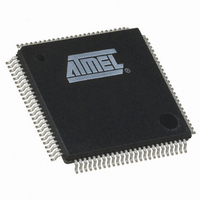
AT91SAM7A3-AU Atmel, AT91SAM7A3-AU Datasheet - Page 157

AT91SAM7A3-AU
Manufacturer Part Number
AT91SAM7A3-AU
Description
IC ARM7 MCU FLASH 256K 100LQFP
Manufacturer
Atmel
Series
AT91SAMr
Specifications of AT91SAM7A3-AU
Core Processor
ARM7
Core Size
16/32-Bit
Speed
60MHz
Connectivity
CAN, I²C, MMC, SPI, SSC, UART/USART
Peripherals
POR, PWM, WDT
Number Of I /o
62
Program Memory Size
256KB (256K x 8)
Program Memory Type
FLASH
Ram Size
32K x 8
Voltage - Supply (vcc/vdd)
1.65 V ~ 1.95 V
Data Converters
A/D 8x10b
Oscillator Type
Internal
Operating Temperature
-40°C ~ 85°C
Package / Case
100-LQFP
Controller Family/series
AT91SAM7xx
No. Of I/o's
62
Ram Memory Size
32KB
Cpu Speed
60MHz
No. Of Timers
3
Rohs Compliant
Yes
Package
100LQFP
Device Core
ARM7TDMI
Family Name
91S
Maximum Speed
60 MHz
Operating Supply Voltage
3.3 V
Data Bus Width
32 Bit
Number Of Programmable I/os
62
Interface Type
CAN/SPI/I2S/TWI/USART/USB
On-chip Adc
2(8-chx10-bit)
Number Of Timers
3
Processor Series
AT91SAMx
Core
ARM7TDMI
Data Ram Size
32 KB
Maximum Clock Frequency
60 MHz
Maximum Operating Temperature
+ 85 C
Mounting Style
SMD/SMT
3rd Party Development Tools
JTRACE-ARM-2M, MDK-ARM, RL-ARM, ULINK2
Development Tools By Supplier
AT91SAM-ICE, AT91-ISP, AT91SAM7A3-EK
Minimum Operating Temperature
- 40 C
Cpu Family
91S
Device Core Size
32b
Frequency (max)
60MHz
Total Internal Ram Size
32KB
# I/os (max)
62
Number Of Timers - General Purpose
3
Operating Supply Voltage (typ)
3.3V
Operating Supply Voltage (max)
3.6V
Operating Supply Voltage (min)
3V
Instruction Set Architecture
RISC
Operating Temp Range
-40C to 85C
Operating Temperature Classification
Industrial
Mounting
Surface Mount
Pin Count
100
Package Type
LQFP
For Use With
AT91SAM-ICE - EMULATOR FOR AT91 ARM7/ARM9AT91SAM7A3-EK - KIT EVAL FOR AT91SAM7A3
Lead Free Status / RoHS Status
Lead free / RoHS Compliant
Eeprom Size
-
Lead Free Status / Rohs Status
Details
Available stocks
Company
Part Number
Manufacturer
Quantity
Price
Company:
Part Number:
AT91SAM7A3-AU
Manufacturer:
MXIC
Quantity:
1 001
Company:
Part Number:
AT91SAM7A3-AU
Manufacturer:
Atmel
Quantity:
730
- Current page: 157 of 594
- Download datasheet (7Mb)
24.6
24.7
6042E–ATARM–14-Dec-06
Programmable Clock Output Controller
Programming Sequence
The bit number within the Peripheral Clock Control registers (PMC_PCER, PMC_PCDR, and
PMC_PCSR) is the Peripheral Identifier defined at the product level. Generally, the bit number
corresponds to the interrupt source number assigned to the peripheral.
The PMC controls 4 signals to be output on external pins PCKx. Each signal can be indepen-
dently programmed via the PMC_PCKx registers.
PCKx can be independently selected between the Slow clock, the PLL output and the main
clock by writing the CSS field in PMC_PCKx. Each output signal can also be divided by a power
of 2 between 1 and 64 by writing the PRES (Prescaler) field in PMC_PCKx.
Each output signal can be enabled and disabled by writing 1 in the corresponding bit, PCKx of
PMC_SCER and PMC_SCDR, respectively. Status of the active programmable output clocks
are given in the PCKx bits of PMC_SCSR (System Clock Status Register).
Moreover, like the PCK, a status bitin PMC_SR indicates that the Programmable Clock is actu-
ally what has been programmed in the Programmable Clock registers.
As the Programmable Clock Controller does not manage with glitch prevention when switching
clocks, it is strongly recommended to disable the Programmable Clock before any configuration
change and to re-enable it after the change is actually performed.
1. Enabling the Main Oscillator:
2. Checking the Main Oscillator Frequency (Optional):
3. Setting PLL and divider:
The main oscillator is enabled by setting the MOSCEN field in the CKGR_MOR register. In
some cases it may be advantageous to define a start-up time. This can be achieved by writ-
ing a value in the OSCOUNT field in the CKGR_MOR register.
Once this register has been correctly configured, the user must wait for MOSCS field in the
PMC_SR register to be set. This can be done either by polling the status register or by wait-
ing the interrupt line to be raised if the associated interrupt to MOSCS has been enabled in
the PMC_IER register.
Code Example:
Start Up Time = 8 * OSCOUNT / SLCK = 56 Slow Clock Cycles.
So, the main oscillator will be enabled (MOSCS bit set) after 56 Slow Clock Cycles.
In some situations the user may need an accurate measure of the main oscillator frequency.
This measure can be accomplished via the CKGR_MCFR register.
Once the MAINRDY field is set in CKGR_MCFR register, the user may read the MAINF field
in CKGR_MCFR register. This provides the number of main clock cycles within sixteen slow
clock cycles.
write_register(CKGR_MOR,0x00000701)
AT91SAM7A3 Preliminary
157
Related parts for AT91SAM7A3-AU
Image
Part Number
Description
Manufacturer
Datasheet
Request
R

Part Number:
Description:
MCU ARM9 64K SRAM 144-LFBGA
Manufacturer:
Atmel
Datasheet:

Part Number:
Description:
IC ARM9 MPU 217-LFBGA
Manufacturer:
Atmel
Datasheet:

Part Number:
Description:
MCU ARM9 ULTRA LOW PWR 217-LFBGA
Manufacturer:
Atmel
Datasheet:

Part Number:
Description:
MCU ARM9 324-TFBGA
Manufacturer:
Atmel
Datasheet:

Part Number:
Description:
IC MCU ARM9 SAMPLING 217CBGA
Manufacturer:
Atmel
Datasheet:

Part Number:
Description:
IC ARM9 MCU 217-LFBGA
Manufacturer:
Atmel
Datasheet:

Part Number:
Description:
IC ARM9 MCU 208-PQFP
Manufacturer:
Atmel
Datasheet:

Part Number:
Description:
MCU ARM 512K HS FLASH 100-LQFP
Manufacturer:
Atmel
Datasheet:

Part Number:
Description:
MCU ARM 512K HS FLASH 100-TFBGA
Manufacturer:
Atmel
Datasheet:

Part Number:
Description:
IC ARM9 MCU 200 MHZ 324-TFBGA
Manufacturer:
Atmel
Datasheet:

Part Number:
Description:
IC ARM MCU 16BIT 128K 256BGA
Manufacturer:
Atmel
Datasheet:

Part Number:
Description:
IC ARM7 MCU 32BIT 128K 64LQFP
Manufacturer:
Atmel
Datasheet:

Part Number:
Description:
IC ARM7 MCU FLASH 256K 128-LQFP
Manufacturer:
Atmel
Datasheet:

Part Number:
Description:
IC ARM7 MCU FLASH 512K 128-LQFP
Manufacturer:
Atmel
Datasheet:

Part Number:
Description:
IC ARM9 MPU 217-LFBGA
Manufacturer:
Atmel
Datasheet:


