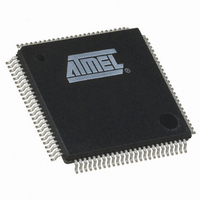
AT91SAM7A3-AU Atmel, AT91SAM7A3-AU Datasheet - Page 423

AT91SAM7A3-AU
Manufacturer Part Number
AT91SAM7A3-AU
Description
IC ARM7 MCU FLASH 256K 100LQFP
Manufacturer
Atmel
Series
AT91SAMr
Specifications of AT91SAM7A3-AU
Core Processor
ARM7
Core Size
16/32-Bit
Speed
60MHz
Connectivity
CAN, I²C, MMC, SPI, SSC, UART/USART
Peripherals
POR, PWM, WDT
Number Of I /o
62
Program Memory Size
256KB (256K x 8)
Program Memory Type
FLASH
Ram Size
32K x 8
Voltage - Supply (vcc/vdd)
1.65 V ~ 1.95 V
Data Converters
A/D 8x10b
Oscillator Type
Internal
Operating Temperature
-40°C ~ 85°C
Package / Case
100-LQFP
Controller Family/series
AT91SAM7xx
No. Of I/o's
62
Ram Memory Size
32KB
Cpu Speed
60MHz
No. Of Timers
3
Rohs Compliant
Yes
Package
100LQFP
Device Core
ARM7TDMI
Family Name
91S
Maximum Speed
60 MHz
Operating Supply Voltage
3.3 V
Data Bus Width
32 Bit
Number Of Programmable I/os
62
Interface Type
CAN/SPI/I2S/TWI/USART/USB
On-chip Adc
2(8-chx10-bit)
Number Of Timers
3
Processor Series
AT91SAMx
Core
ARM7TDMI
Data Ram Size
32 KB
Maximum Clock Frequency
60 MHz
Maximum Operating Temperature
+ 85 C
Mounting Style
SMD/SMT
3rd Party Development Tools
JTRACE-ARM-2M, MDK-ARM, RL-ARM, ULINK2
Development Tools By Supplier
AT91SAM-ICE, AT91-ISP, AT91SAM7A3-EK
Minimum Operating Temperature
- 40 C
Cpu Family
91S
Device Core Size
32b
Frequency (max)
60MHz
Total Internal Ram Size
32KB
# I/os (max)
62
Number Of Timers - General Purpose
3
Operating Supply Voltage (typ)
3.3V
Operating Supply Voltage (max)
3.6V
Operating Supply Voltage (min)
3V
Instruction Set Architecture
RISC
Operating Temp Range
-40C to 85C
Operating Temperature Classification
Industrial
Mounting
Surface Mount
Pin Count
100
Package Type
LQFP
For Use With
AT91SAM-ICE - EMULATOR FOR AT91 ARM7/ARM9AT91SAM7A3-EK - KIT EVAL FOR AT91SAM7A3
Lead Free Status / RoHS Status
Lead free / RoHS Compliant
Eeprom Size
-
Lead Free Status / Rohs Status
Details
Available stocks
Company
Part Number
Manufacturer
Quantity
Price
Company:
Part Number:
AT91SAM7A3-AU
Manufacturer:
MXIC
Quantity:
1 001
Company:
Part Number:
AT91SAM7A3-AU
Manufacturer:
Atmel
Quantity:
730
- Current page: 423 of 594
- Download datasheet (7Mb)
Figure 33-11. Data OUT Transfer for Ping-pong Endpoint
Note:
33.5.2.8
6042E–ATARM–14-Dec-06
USB Bus
Packets
RX_DATA_BK0 Flag
(UDP_CSRx)
RX_DATA_BK1 Flag
(UDP_CSRx)
FIFO (DPR)
Bank 0
FIFO (DPR)
Bank 1
An interrupt is pending while the RX_DATA_BK0 or RX_DATA_BK1 flag is set.
Stall Handshake
Host Sends First Data Payload
Data OUT
PID
Set by USB Device,
Data Payload Written
in FIFO Endpoint Bank 0
Write by USB Device
Data OUT1
Warning: When RX_DATA_BK0 and RX_DATA_BK1 are both set, there is no way to determine
which one to clear first. Thus the software must keep an internal counter to be sure to clear alter-
natively RX_DATA_BK0 then RX_DATA_BK1. This situation may occur when the software
application is busy elsewhere and the two banks are filled by the USB host. Once the application
comes back to the USB driver, the two flags are set.
A stall handshake can be used in one of two distinct occasions. (For more information on the
stall handshake, refer to Chapter 8 of the Universal Serial Bus Specification, Rev 2.0.)
The following procedure generates a stall packet:
10. The microcontroller transfers out data received from the endpoint’s memory to the
11. The microcontroller notifies the USB device it has finished the transfer by clearing
12. A fourth Data OUT packet can be accepted by the USB device and copied in the FIFO
• A functional stall is used when the halt feature associated with the endpoint is set. (Refer to
• To abort the current request, a protocol stall is used, but uniquely with control transfer.
Chapter 9 of the Universal Serial Bus Specification, Rev 2.0, for more information on the halt
feature.)
microcontroller’s memory. Data received is available by reading the endpoint’s UDP_
FDRx register.
RX_DATA_BK1 in the endpoint’s UDP_ CSRx register.
Bank 0.
Data OUT 1
ACK
PID
Read By Microcontroller
Set by USB Device,
Data Payload Written
in FIFO Endpoint Bank 1
Interrupt Pending
Microcontroller Reads Data 1 in Bank 0,
Host Sends Second Data Payload
Data OUT 1
Data OUT
PID
Write by USB Device
Data OUT 2
Data OUT 2
AT91SAM7A3 Preliminary
Cleared by Firmware
ACK
PID
Read By Microcontroller
Microcontroller Reads Data2 in Bank 1,
Host Sends Third Data Payload
Data OUT
PID
Interrupt Pending
Data OUT 2
Write In Progress
Cleared by Firmware
Data OUT 3
Data OUT 3
A
P
423
Related parts for AT91SAM7A3-AU
Image
Part Number
Description
Manufacturer
Datasheet
Request
R

Part Number:
Description:
MCU ARM9 64K SRAM 144-LFBGA
Manufacturer:
Atmel
Datasheet:

Part Number:
Description:
IC ARM9 MPU 217-LFBGA
Manufacturer:
Atmel
Datasheet:

Part Number:
Description:
MCU ARM9 ULTRA LOW PWR 217-LFBGA
Manufacturer:
Atmel
Datasheet:

Part Number:
Description:
MCU ARM9 324-TFBGA
Manufacturer:
Atmel
Datasheet:

Part Number:
Description:
IC MCU ARM9 SAMPLING 217CBGA
Manufacturer:
Atmel
Datasheet:

Part Number:
Description:
IC ARM9 MCU 217-LFBGA
Manufacturer:
Atmel
Datasheet:

Part Number:
Description:
IC ARM9 MCU 208-PQFP
Manufacturer:
Atmel
Datasheet:

Part Number:
Description:
MCU ARM 512K HS FLASH 100-LQFP
Manufacturer:
Atmel
Datasheet:

Part Number:
Description:
MCU ARM 512K HS FLASH 100-TFBGA
Manufacturer:
Atmel
Datasheet:

Part Number:
Description:
IC ARM9 MCU 200 MHZ 324-TFBGA
Manufacturer:
Atmel
Datasheet:

Part Number:
Description:
IC ARM MCU 16BIT 128K 256BGA
Manufacturer:
Atmel
Datasheet:

Part Number:
Description:
IC ARM7 MCU 32BIT 128K 64LQFP
Manufacturer:
Atmel
Datasheet:

Part Number:
Description:
IC ARM7 MCU FLASH 256K 128-LQFP
Manufacturer:
Atmel
Datasheet:

Part Number:
Description:
IC ARM7 MCU FLASH 512K 128-LQFP
Manufacturer:
Atmel
Datasheet:

Part Number:
Description:
IC ARM9 MPU 217-LFBGA
Manufacturer:
Atmel
Datasheet:


