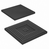
AT91SAM9XE512-CU Atmel, AT91SAM9XE512-CU Datasheet - Page 179

AT91SAM9XE512-CU
Manufacturer Part Number
AT91SAM9XE512-CU
Description
MCU ARM9 512K FLASH 217-BGA
Manufacturer
Atmel
Series
AT91SAMr
Datasheet
1.AT91SAM9XE128-QU.pdf
(860 pages)
Specifications of AT91SAM9XE512-CU
Core Processor
ARM9
Core Size
16/32-Bit
Speed
180MHz
Connectivity
EBI/EMI, Ethernet, I²C, MMC, SPI, SSC, UART/USART, USB
Peripherals
Brown-out Detect/Reset, POR, PWM, WDT
Number Of I /o
96
Program Memory Size
512KB (512K x 8)
Program Memory Type
FLASH
Ram Size
56K x 8
Voltage - Supply (vcc/vdd)
1.65 V ~ 1.95 V
Data Converters
A/D 4x10b
Oscillator Type
Internal
Operating Temperature
-40°C ~ 85°C
Package / Case
217-LFBGA
Package
217LFBGA
Device Core
ARM926EJ-S
Family Name
91S
Maximum Speed
180 MHz
Operating Supply Voltage
1.8|2.5|3.3 V
Data Bus Width
32 Bit
Number Of Programmable I/os
96
Interface Type
EBI/Ethernet/SPI/TWI/USART/USB
On-chip Adc
4-chx10-bit
Number Of Timers
6
Processor Series
AT91SAMx
Core
ARM926EJ-S
Data Ram Size
32 KB
Maximum Clock Frequency
180 MHz
Maximum Operating Temperature
+ 85 C
Mounting Style
SMD/SMT
3rd Party Development Tools
JTRACE-ARM-2M, KSK-AT91SAM9XE-PL, MDK-ARM, RL-ARM, ULINK2
Development Tools By Supplier
AT91SAM-ICE, AT91-ISP, AT91SAM9XE-EK
Minimum Operating Temperature
- 40 C
For Use With
AT91SAM9XE-EK - KIT EVAL FOR AT91SAM9XEAT91SAM-ICE - EMULATOR FOR AT91 ARM7/ARM9
Lead Free Status / RoHS Status
Lead free / RoHS Compliant
Eeprom Size
-
Lead Free Status / Rohs Status
Details
Available stocks
Company
Part Number
Manufacturer
Quantity
Price
Company:
Part Number:
AT91SAM9XE512-CU
Manufacturer:
NEC
Quantity:
201
Part Number:
AT91SAM9XE512-CU
Manufacturer:
ATMEL/爱特梅尔
Quantity:
20 000
- Current page: 179 of 860
- Download datasheet (13Mb)
Table 22-6.
22.6.6.3
6254C–ATARM–22-Jan-10
Mode
Attribute Memory
Common Memory
I/O Mode
True IDE Mode
Alternate True IDE Mode
Standby Mode or
Address Space is not
assigned to CF
Alternate Status Read
Control Register
Drive Address
Data Register
Read/Write Signals
Task File
CFCE1 and CFCE2 Truth Table
The CFCE1 and CFCE2 waveforms are identical to the corresponding NCSx waveform. For
details on these waveforms and timings, refer to the Static Memory Controller section.
In I/O mode and True IDE mode, the CompactFlash logic drives the read and write command
signals of the SMC on CFIOR and CFIOW signals, while the CFOE and CFWE signals are deac-
tivated. Likewise, in common memory mode and attribute memory mode, the SMC signals are
driven on the CFOE and CFWE signals, while the CFIOR and CFIOW are deactivated.
22-4 on page 180
Attribute memory mode, common memory mode and I/O mode are supported by setting the
address setup and hold time on the NCS4 (and/or NCS5) chip select to the appropriate values.
CFCE2
NBS1
NBS1
NBS1
1
1
1
1
0
0
1
CFCE1
demonstrates a schematic representation of this logic.
NBS0
NBS0
NBS0
0
0
0
0
1
1
1
AT91SAM9XE128/256/512 Preliminary
16 bits
16 bits
16 bits
16bits
DBW
8 bits
8 bits
8 bits
Don’t
8 bits
Care
–
Comment
Access to Even Byte on D[7:0]
Access to Even Byte on D[7:0]
Access to Odd Byte on D[15:8]
Access to Odd Byte on D[7:0]
Access to Even Byte on D[7:0]
Access to Odd Byte on D[15:8]
Access to Odd Byte on D[7:0]
Access to Even Byte on D[7:0]
Access to Odd Byte on D[7:0]
Access to Even Byte on D[7:0]
Access to Odd Byte on D[15:8]
Access to Even Byte on D[7:0]
Access to Odd Byte on D[7:0]
–
SMC Access Mode
Byte Select
Byte Select
Byte Select
Byte Select
Don’t Care
–
Figure
179
Related parts for AT91SAM9XE512-CU
Image
Part Number
Description
Manufacturer
Datasheet
Request
R

Part Number:
Description:
KIT EVAL FOR AT91SAM9XE
Manufacturer:
Atmel
Datasheet:

Part Number:
Description:
MCU ARM9 64K SRAM 144-LFBGA
Manufacturer:
Atmel
Datasheet:

Part Number:
Description:
IC ARM7 MCU FLASH 256K 100LQFP
Manufacturer:
Atmel
Datasheet:

Part Number:
Description:
IC ARM9 MPU 217-LFBGA
Manufacturer:
Atmel
Datasheet:

Part Number:
Description:
MCU ARM9 ULTRA LOW PWR 217-LFBGA
Manufacturer:
Atmel
Datasheet:

Part Number:
Description:
MCU ARM9 324-TFBGA
Manufacturer:
Atmel
Datasheet:

Part Number:
Description:
IC MCU ARM9 SAMPLING 217CBGA
Manufacturer:
Atmel
Datasheet:

Part Number:
Description:
IC ARM9 MCU 217-LFBGA
Manufacturer:
Atmel
Datasheet:

Part Number:
Description:
IC ARM9 MCU 208-PQFP
Manufacturer:
Atmel
Datasheet:

Part Number:
Description:
MCU ARM 512K HS FLASH 100-LQFP
Manufacturer:
Atmel
Datasheet:

Part Number:
Description:
MCU ARM 512K HS FLASH 100-TFBGA
Manufacturer:
Atmel
Datasheet:

Part Number:
Description:
IC ARM9 MCU 200 MHZ 324-TFBGA
Manufacturer:
Atmel
Datasheet:

Part Number:
Description:
IC ARM MCU 16BIT 128K 256BGA
Manufacturer:
Atmel
Datasheet:

Part Number:
Description:
IC ARM7 MCU 32BIT 128K 64LQFP
Manufacturer:
Atmel
Datasheet:

Part Number:
Description:
IC ARM7 MCU FLASH 256K 128-LQFP
Manufacturer:
Atmel
Datasheet:


