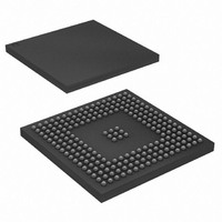
AT91SAM9XE512-CU Atmel, AT91SAM9XE512-CU Datasheet - Page 86

AT91SAM9XE512-CU
Manufacturer Part Number
AT91SAM9XE512-CU
Description
MCU ARM9 512K FLASH 217-BGA
Manufacturer
Atmel
Series
AT91SAMr
Datasheet
1.AT91SAM9XE128-QU.pdf
(860 pages)
Specifications of AT91SAM9XE512-CU
Core Processor
ARM9
Core Size
16/32-Bit
Speed
180MHz
Connectivity
EBI/EMI, Ethernet, I²C, MMC, SPI, SSC, UART/USART, USB
Peripherals
Brown-out Detect/Reset, POR, PWM, WDT
Number Of I /o
96
Program Memory Size
512KB (512K x 8)
Program Memory Type
FLASH
Ram Size
56K x 8
Voltage - Supply (vcc/vdd)
1.65 V ~ 1.95 V
Data Converters
A/D 4x10b
Oscillator Type
Internal
Operating Temperature
-40°C ~ 85°C
Package / Case
217-LFBGA
Package
217LFBGA
Device Core
ARM926EJ-S
Family Name
91S
Maximum Speed
180 MHz
Operating Supply Voltage
1.8|2.5|3.3 V
Data Bus Width
32 Bit
Number Of Programmable I/os
96
Interface Type
EBI/Ethernet/SPI/TWI/USART/USB
On-chip Adc
4-chx10-bit
Number Of Timers
6
Processor Series
AT91SAMx
Core
ARM926EJ-S
Data Ram Size
32 KB
Maximum Clock Frequency
180 MHz
Maximum Operating Temperature
+ 85 C
Mounting Style
SMD/SMT
3rd Party Development Tools
JTRACE-ARM-2M, KSK-AT91SAM9XE-PL, MDK-ARM, RL-ARM, ULINK2
Development Tools By Supplier
AT91SAM-ICE, AT91-ISP, AT91SAM9XE-EK
Minimum Operating Temperature
- 40 C
For Use With
AT91SAM9XE-EK - KIT EVAL FOR AT91SAM9XEAT91SAM-ICE - EMULATOR FOR AT91 ARM7/ARM9
Lead Free Status / RoHS Status
Lead free / RoHS Compliant
Eeprom Size
-
Lead Free Status / Rohs Status
Details
Available stocks
Company
Part Number
Manufacturer
Quantity
Price
Company:
Part Number:
AT91SAM9XE512-CU
Manufacturer:
NEC
Quantity:
201
Part Number:
AT91SAM9XE512-CU
Manufacturer:
ATMEL/爱特梅尔
Quantity:
20 000
- Current page: 86 of 860
- Download datasheet (13Mb)
Table 14-1.
14.2.2
86
Signal Name
XIN
TST
PGMEN0
PGMEN1
PGMEN2
PGMEN3
PGMNCMD
PGMRDY
PGMNOE
PGMNVALID
PGMM[3:0]
PGMD[15:0]
AT91SAM9XE128/256/512 Preliminary
Signal Names
Signal Description List (Continued)
Function
Main Clock Input.
This input can be tied to GND. In this
case, the device is clocked by the internal
RC oscillator.
Test Mode Select
Test Mode Select
Test Mode Select
Test Mode Select
Test Mode Select
Valid command available
0: Device is busy
1: Device is ready for a new command
Output Enable (active high)
0: DATA[15:0] is in input mode
1: DATA[15:0] is in output mode
Specifies DATA type (See
Bi-directional data bus
Depending on the MODE settings, DATA is latched in different internal registers.
Table 14-2.
When MODE is equal to CMDE, then a new command (strobed on DATA[15:0] signals) is stored
in the command register.
MODE[3:0]
0000
0001
0010
0011
0100
0101
Default
Mode Coding
Table
Symbol
CMDE
ADDR0
ADDR1
ADDR2
ADDR3
DATA
IDLE
14-2)
Clocks
Test
PIO
Input/Output
Output
Output
Type
Input
Input
Input
Input
Input
Input
Input
Input
Input
Data
Command Register
No register
Address Register LSBs
Address Register MSBs
Data Register
Active
Level
High
High
High
High
Low
Low
Low
Low
Low
Comments
32KHz to 50MHz
Must be connected to VDDBU
Must be connected to VDDIO
Must be connected to VDDIO
Must be connected to GND
Must be connected to GND
Pulled-up input at reset
Pulled-up input at reset
Pulled-up input at reset
Pulled-up input at reset
Pulled-up input at reset
Pulled-up input at reset
6254C–ATARM–22-Jan-10
Related parts for AT91SAM9XE512-CU
Image
Part Number
Description
Manufacturer
Datasheet
Request
R

Part Number:
Description:
KIT EVAL FOR AT91SAM9XE
Manufacturer:
Atmel
Datasheet:

Part Number:
Description:
MCU ARM9 64K SRAM 144-LFBGA
Manufacturer:
Atmel
Datasheet:

Part Number:
Description:
IC ARM7 MCU FLASH 256K 100LQFP
Manufacturer:
Atmel
Datasheet:

Part Number:
Description:
IC ARM9 MPU 217-LFBGA
Manufacturer:
Atmel
Datasheet:

Part Number:
Description:
MCU ARM9 ULTRA LOW PWR 217-LFBGA
Manufacturer:
Atmel
Datasheet:

Part Number:
Description:
MCU ARM9 324-TFBGA
Manufacturer:
Atmel
Datasheet:

Part Number:
Description:
IC MCU ARM9 SAMPLING 217CBGA
Manufacturer:
Atmel
Datasheet:

Part Number:
Description:
IC ARM9 MCU 217-LFBGA
Manufacturer:
Atmel
Datasheet:

Part Number:
Description:
IC ARM9 MCU 208-PQFP
Manufacturer:
Atmel
Datasheet:

Part Number:
Description:
MCU ARM 512K HS FLASH 100-LQFP
Manufacturer:
Atmel
Datasheet:

Part Number:
Description:
MCU ARM 512K HS FLASH 100-TFBGA
Manufacturer:
Atmel
Datasheet:

Part Number:
Description:
IC ARM9 MCU 200 MHZ 324-TFBGA
Manufacturer:
Atmel
Datasheet:

Part Number:
Description:
IC ARM MCU 16BIT 128K 256BGA
Manufacturer:
Atmel
Datasheet:

Part Number:
Description:
IC ARM7 MCU 32BIT 128K 64LQFP
Manufacturer:
Atmel
Datasheet:

Part Number:
Description:
IC ARM7 MCU FLASH 256K 128-LQFP
Manufacturer:
Atmel
Datasheet:


