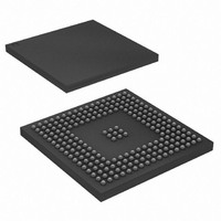
AT91SAM9XE512-CU Atmel, AT91SAM9XE512-CU Datasheet - Page 560

AT91SAM9XE512-CU
Manufacturer Part Number
AT91SAM9XE512-CU
Description
MCU ARM9 512K FLASH 217-BGA
Manufacturer
Atmel
Series
AT91SAMr
Datasheet
1.AT91SAM9XE128-QU.pdf
(860 pages)
Specifications of AT91SAM9XE512-CU
Core Processor
ARM9
Core Size
16/32-Bit
Speed
180MHz
Connectivity
EBI/EMI, Ethernet, I²C, MMC, SPI, SSC, UART/USART, USB
Peripherals
Brown-out Detect/Reset, POR, PWM, WDT
Number Of I /o
96
Program Memory Size
512KB (512K x 8)
Program Memory Type
FLASH
Ram Size
56K x 8
Voltage - Supply (vcc/vdd)
1.65 V ~ 1.95 V
Data Converters
A/D 4x10b
Oscillator Type
Internal
Operating Temperature
-40°C ~ 85°C
Package / Case
217-LFBGA
Package
217LFBGA
Device Core
ARM926EJ-S
Family Name
91S
Maximum Speed
180 MHz
Operating Supply Voltage
1.8|2.5|3.3 V
Data Bus Width
32 Bit
Number Of Programmable I/os
96
Interface Type
EBI/Ethernet/SPI/TWI/USART/USB
On-chip Adc
4-chx10-bit
Number Of Timers
6
Processor Series
AT91SAMx
Core
ARM926EJ-S
Data Ram Size
32 KB
Maximum Clock Frequency
180 MHz
Maximum Operating Temperature
+ 85 C
Mounting Style
SMD/SMT
3rd Party Development Tools
JTRACE-ARM-2M, KSK-AT91SAM9XE-PL, MDK-ARM, RL-ARM, ULINK2
Development Tools By Supplier
AT91SAM-ICE, AT91-ISP, AT91SAM9XE-EK
Minimum Operating Temperature
- 40 C
For Use With
AT91SAM9XE-EK - KIT EVAL FOR AT91SAM9XEAT91SAM-ICE - EMULATOR FOR AT91 ARM7/ARM9
Lead Free Status / RoHS Status
Lead free / RoHS Compliant
Eeprom Size
-
Lead Free Status / Rohs Status
Details
Available stocks
Company
Part Number
Manufacturer
Quantity
Price
Company:
Part Number:
AT91SAM9XE512-CU
Manufacturer:
NEC
Quantity:
201
Part Number:
AT91SAM9XE512-CU
Manufacturer:
ATMEL/爱特梅尔
Quantity:
20 000
- Current page: 560 of 860
- Download datasheet (13Mb)
35.6.6.1
35.6.7
Table 35-3.
560
Transmitter
SSC_TFMR
SSC_TFMR
SSC_TFMR
SSC_TFMR
SSC_TFMR
SSC_TFMR
SSC_TCMR
SSC_TCMR
AT91SAM9XE128/256/512 Preliminary
Data Format
Compare Functions
Data Frame Registers
Receiver
SSC_RFMR
SSC_RFMR
SSC_RFMR
SSC_RFMR
SSC_RCMR
SSC_RCMR
Length of the comparison patterns (Compare 0, Compare 1) and thus the number of bits they
are compared to is defined by FSLEN, but with a maximum value of 16 bits. Comparison is
always done by comparing the last bits received with the comparison pattern. Compare 0 can be
one start event of the Receiver. In this case, the receiver compares at each new sample the last
bits received at the Compare 0 pattern contained in the Compare 0 Register (SSC_RC0R).
When this start event is selected, the user can program the Receiver to start a new data transfer
either by writing a new Compare 0, or by receiving continuously until Compare 1 occurs. This
selection is done with the bit (STOP) in SSC_RCMR.
The data framing format of both the transmitter and the receiver are programmable through the
Transmitter Frame Mode Register (SSC_TFMR) and the Receiver Frame Mode Register
(SSC_RFMR). In either case, the user can independently select:
Additionally, the transmitter can be used to transfer synchronization and select the level driven
on the TD pin while not in data transfer operation. This is done respectively by the Frame Sync
Data Enable (FSDEN) and by the Data Default Value (DATDEF) bits in SSC_TFMR.
• the event that starts the data transfer (START)
• the delay in number of bit periods between the start event and the first data bit (STTDLY)
• the length of the data (DATLEN)
• the number of data to be transferred for each start event (DATNB).
• the length of synchronization transferred for each start event (FSLEN)
• the bit sense: most or lowest significant bit first (MSBF)
Field
DATLEN
DATNB
MSBF
FSLEN
DATDEF
FSDEN
PERIOD
STTDLY
Length
Up to 32
Up to 16
Up to 16
0 or 1
Up to 512
Up to 255
Comment
Size of word
Number of words transmitted in frame
Most significant bit first
Size of Synchro data register
Data default value ended
Enable send SSC_TSHR
Frame size
Size of transmit start delay
6254C–ATARM–22-Jan-10
Related parts for AT91SAM9XE512-CU
Image
Part Number
Description
Manufacturer
Datasheet
Request
R

Part Number:
Description:
KIT EVAL FOR AT91SAM9XE
Manufacturer:
Atmel
Datasheet:

Part Number:
Description:
MCU ARM9 64K SRAM 144-LFBGA
Manufacturer:
Atmel
Datasheet:

Part Number:
Description:
IC ARM7 MCU FLASH 256K 100LQFP
Manufacturer:
Atmel
Datasheet:

Part Number:
Description:
IC ARM9 MPU 217-LFBGA
Manufacturer:
Atmel
Datasheet:

Part Number:
Description:
MCU ARM9 ULTRA LOW PWR 217-LFBGA
Manufacturer:
Atmel
Datasheet:

Part Number:
Description:
MCU ARM9 324-TFBGA
Manufacturer:
Atmel
Datasheet:

Part Number:
Description:
IC MCU ARM9 SAMPLING 217CBGA
Manufacturer:
Atmel
Datasheet:

Part Number:
Description:
IC ARM9 MCU 217-LFBGA
Manufacturer:
Atmel
Datasheet:

Part Number:
Description:
IC ARM9 MCU 208-PQFP
Manufacturer:
Atmel
Datasheet:

Part Number:
Description:
MCU ARM 512K HS FLASH 100-LQFP
Manufacturer:
Atmel
Datasheet:

Part Number:
Description:
MCU ARM 512K HS FLASH 100-TFBGA
Manufacturer:
Atmel
Datasheet:

Part Number:
Description:
IC ARM9 MCU 200 MHZ 324-TFBGA
Manufacturer:
Atmel
Datasheet:

Part Number:
Description:
IC ARM MCU 16BIT 128K 256BGA
Manufacturer:
Atmel
Datasheet:

Part Number:
Description:
IC ARM7 MCU 32BIT 128K 64LQFP
Manufacturer:
Atmel
Datasheet:

Part Number:
Description:
IC ARM7 MCU FLASH 256K 128-LQFP
Manufacturer:
Atmel
Datasheet:


