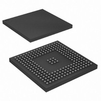
AT91SAM9XE512-CU Atmel, AT91SAM9XE512-CU Datasheet - Page 25

AT91SAM9XE512-CU
Manufacturer Part Number
AT91SAM9XE512-CU
Description
MCU ARM9 512K FLASH 217-BGA
Manufacturer
Atmel
Series
AT91SAMr
Datasheet
1.AT91SAM9XE128-QU.pdf
(860 pages)
Specifications of AT91SAM9XE512-CU
Core Processor
ARM9
Core Size
16/32-Bit
Speed
180MHz
Connectivity
EBI/EMI, Ethernet, I²C, MMC, SPI, SSC, UART/USART, USB
Peripherals
Brown-out Detect/Reset, POR, PWM, WDT
Number Of I /o
96
Program Memory Size
512KB (512K x 8)
Program Memory Type
FLASH
Ram Size
56K x 8
Voltage - Supply (vcc/vdd)
1.65 V ~ 1.95 V
Data Converters
A/D 4x10b
Oscillator Type
Internal
Operating Temperature
-40°C ~ 85°C
Package / Case
217-LFBGA
Package
217LFBGA
Device Core
ARM926EJ-S
Family Name
91S
Maximum Speed
180 MHz
Operating Supply Voltage
1.8|2.5|3.3 V
Data Bus Width
32 Bit
Number Of Programmable I/os
96
Interface Type
EBI/Ethernet/SPI/TWI/USART/USB
On-chip Adc
4-chx10-bit
Number Of Timers
6
Processor Series
AT91SAMx
Core
ARM926EJ-S
Data Ram Size
32 KB
Maximum Clock Frequency
180 MHz
Maximum Operating Temperature
+ 85 C
Mounting Style
SMD/SMT
3rd Party Development Tools
JTRACE-ARM-2M, KSK-AT91SAM9XE-PL, MDK-ARM, RL-ARM, ULINK2
Development Tools By Supplier
AT91SAM-ICE, AT91-ISP, AT91SAM9XE-EK
Minimum Operating Temperature
- 40 C
For Use With
AT91SAM9XE-EK - KIT EVAL FOR AT91SAM9XEAT91SAM-ICE - EMULATOR FOR AT91 ARM7/ARM9
Lead Free Status / RoHS Status
Lead free / RoHS Compliant
Eeprom Size
-
Lead Free Status / Rohs Status
Details
Available stocks
Company
Part Number
Manufacturer
Quantity
Price
Company:
Part Number:
AT91SAM9XE512-CU
Manufacturer:
NEC
Quantity:
201
Part Number:
AT91SAM9XE512-CU
Manufacturer:
ATMEL/爱特梅尔
Quantity:
20 000
- Current page: 25 of 860
- Download datasheet (13Mb)
8.1.5.5
8.1.6
8.1.6.1
6254C–ATARM–22-Jan-10
Boot Strategies
Non-volatile Brownout Detector Control
GPNVMBit[3] = 0, Boot on Embedded ROM
Two GPNVM bits are used for controlling the brownout detector (BOD), so that even after a
power loss, the brownout detector operations remain in their state.
Table 8-3
status and the GPNVMBit[3] state at reset.
Table 8-3.
The system always boots at address 0x0. To ensure a maximum number of possibilities for boot,
the memory layout can be configured with two parameters.
REMAP allows the user to lay out the first internal SRAM bank to 0x0 to ease development. This
is done by software once the system has booted. Refer to the section “AT91SAM9XE Bus
Matrix” in the product datasheet for more details.
When REMAP = 0, a non volatile bit stored in Flash memory (GPNVMBit[3]) allows the user to
lay out to 0x0, at his convenience, the ROM or the Flash. Refer to the section “Enhanced
Embedded Flash Controller (EEFC)” in the product datasheet for more details.
Note:
The AT91SAM9XE Matrix manages a boot memory that depends on the value of GPNVMBit[3]
at reset. The internal memory area mapped between address 0x0 and 0x0FFF FFFF is reserved
for this purpose.
If GPNVMBit[3] is set, the boot memory is the internal Flash memory
If GPNVMBit[3] is clear (Flash reset State), the boot memory is the embedded ROM. After a
Flash erase, the boot memory is the internal ROM.
The system boots using the Boot Program.
0x0000 0000
• GPNVMBit[1] is used as a brownout detector enable bit. Setting GPNVMBit[1] enables the
• GPNVMBit[2] is used as a brownout reset enable signal for the reset controller. Setting
• Boot on slow clock (On-chip RC oscillator or 32,768 Hz low-power oscillator)
• Auto baudrate detection
• SAM-BA Boot in case no valid program is detected in external NVM, supporting
BOD, clearing it disables the BOD. Asserting ERASE clears GPNVMBit[1] and thus disables
the brownout detector by default.
GPNVMBit[2] enables the brownout reset when a brownout is detected, clearing
GPNVMBit[2] disables the brownout reset. Asserting ERASE disables the brownout reset by
default.
– Serial communication on a DBGU
– USB Device Port
Memory blocks not affected by these parameters can always be seen at their specified base
addresses. See the complete memory map presented in
summarizes the Internal Memory Mapping for each Master, depending on the Remap
Address
Internal Memory Mapping
AT91SAM9XE128/256/512 Preliminary
REMAP = 0
GPNVMBit[3] clear
ROM
GPNVMBit[3] set
Flash
Figure 8-1 on page
REMAP = 1
SRAM
20.
25
Related parts for AT91SAM9XE512-CU
Image
Part Number
Description
Manufacturer
Datasheet
Request
R

Part Number:
Description:
KIT EVAL FOR AT91SAM9XE
Manufacturer:
Atmel
Datasheet:

Part Number:
Description:
MCU ARM9 64K SRAM 144-LFBGA
Manufacturer:
Atmel
Datasheet:

Part Number:
Description:
IC ARM7 MCU FLASH 256K 100LQFP
Manufacturer:
Atmel
Datasheet:

Part Number:
Description:
IC ARM9 MPU 217-LFBGA
Manufacturer:
Atmel
Datasheet:

Part Number:
Description:
MCU ARM9 ULTRA LOW PWR 217-LFBGA
Manufacturer:
Atmel
Datasheet:

Part Number:
Description:
MCU ARM9 324-TFBGA
Manufacturer:
Atmel
Datasheet:

Part Number:
Description:
IC MCU ARM9 SAMPLING 217CBGA
Manufacturer:
Atmel
Datasheet:

Part Number:
Description:
IC ARM9 MCU 217-LFBGA
Manufacturer:
Atmel
Datasheet:

Part Number:
Description:
IC ARM9 MCU 208-PQFP
Manufacturer:
Atmel
Datasheet:

Part Number:
Description:
MCU ARM 512K HS FLASH 100-LQFP
Manufacturer:
Atmel
Datasheet:

Part Number:
Description:
MCU ARM 512K HS FLASH 100-TFBGA
Manufacturer:
Atmel
Datasheet:

Part Number:
Description:
IC ARM9 MCU 200 MHZ 324-TFBGA
Manufacturer:
Atmel
Datasheet:

Part Number:
Description:
IC ARM MCU 16BIT 128K 256BGA
Manufacturer:
Atmel
Datasheet:

Part Number:
Description:
IC ARM7 MCU 32BIT 128K 64LQFP
Manufacturer:
Atmel
Datasheet:

Part Number:
Description:
IC ARM7 MCU FLASH 256K 128-LQFP
Manufacturer:
Atmel
Datasheet:


