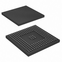
AT91SAM9XE512-CU Atmel, AT91SAM9XE512-CU Datasheet - Page 840

AT91SAM9XE512-CU
Manufacturer Part Number
AT91SAM9XE512-CU
Description
MCU ARM9 512K FLASH 217-BGA
Manufacturer
Atmel
Series
AT91SAMr
Datasheet
1.AT91SAM9XE128-QU.pdf
(860 pages)
Specifications of AT91SAM9XE512-CU
Core Processor
ARM9
Core Size
16/32-Bit
Speed
180MHz
Connectivity
EBI/EMI, Ethernet, I²C, MMC, SPI, SSC, UART/USART, USB
Peripherals
Brown-out Detect/Reset, POR, PWM, WDT
Number Of I /o
96
Program Memory Size
512KB (512K x 8)
Program Memory Type
FLASH
Ram Size
56K x 8
Voltage - Supply (vcc/vdd)
1.65 V ~ 1.95 V
Data Converters
A/D 4x10b
Oscillator Type
Internal
Operating Temperature
-40°C ~ 85°C
Package / Case
217-LFBGA
Package
217LFBGA
Device Core
ARM926EJ-S
Family Name
91S
Maximum Speed
180 MHz
Operating Supply Voltage
1.8|2.5|3.3 V
Data Bus Width
32 Bit
Number Of Programmable I/os
96
Interface Type
EBI/Ethernet/SPI/TWI/USART/USB
On-chip Adc
4-chx10-bit
Number Of Timers
6
Processor Series
AT91SAMx
Core
ARM926EJ-S
Data Ram Size
32 KB
Maximum Clock Frequency
180 MHz
Maximum Operating Temperature
+ 85 C
Mounting Style
SMD/SMT
3rd Party Development Tools
JTRACE-ARM-2M, KSK-AT91SAM9XE-PL, MDK-ARM, RL-ARM, ULINK2
Development Tools By Supplier
AT91SAM-ICE, AT91-ISP, AT91SAM9XE-EK
Minimum Operating Temperature
- 40 C
For Use With
AT91SAM9XE-EK - KIT EVAL FOR AT91SAM9XEAT91SAM-ICE - EMULATOR FOR AT91 ARM7/ARM9
Lead Free Status / RoHS Status
Lead free / RoHS Compliant
Eeprom Size
-
Lead Free Status / Rohs Status
Details
Available stocks
Company
Part Number
Manufacturer
Quantity
Price
Company:
Part Number:
AT91SAM9XE512-CU
Manufacturer:
NEC
Quantity:
201
Part Number:
AT91SAM9XE512-CU
Manufacturer:
ATMEL/爱特梅尔
Quantity:
20 000
- Current page: 840 of 860
- Download datasheet (13Mb)
46.2.6
46.2.6.1
46.2.6.2
46.2.6.3
46.2.7
46.2.7.1
46.2.7.2
840
AT91SAM9XE128/256/512 Preliminary
Serial Peripheral Interface (SPI)
Serial Synchronous Controller (SSC)
SPI: Bad Serial Clock Generation on second chip_select when SCBR = 1, CPOL = 1 and NCPHA = 0
SPI: Software Reset must be Written Twice
SPI: Inaccurate RHR.PCS in Variable Mode
SSC: Transmitter Limitations in Slave Mode
SSC: Delay on TD (transmit data signal)
If the SPI is used in the following configuration:
then an additional pulse will be generated on output SPCK during the second transfer.
Do not use a multiple Chip Select configuration where at least one SCRx register is configured
with SCBR = 1 and the others differ from 1 if CPHA = 0 and CPOL = 1.
If all chip selects are configured with Baudrate = 1, the issue does not appear.
If a software reset (SWRST in the SPI control register) is performed, the SPI may not work prop-
erly (the clock is enabled before the chip select.)
The SPI Control Register field SWRST (Software Reset) needs to be written twice to be correctly
set.
When the SPI is configured in master mode, connected to four slaves and the variable periph-
eral mode is selected, the PCS field in the SPI_RDR does not accurately tell which slave the
received data came from if all Chip Selects are used consecutively.
Use DLYBCT field of the SPI Chip Select Register to include a delay between two consecutive
transfers.
If TK is programmed as output and TF is programmed as input, it is impossible to emit data
when start of edge (rising or falling) of synchro with a Start Delay equal to zero.
None.
When:
• master mode
• CPOL = 1 and NCPHA = 0
• multiple chip selects used with one transfer with Baud rate (SCBR) equal to 1 (i.e., when
• transmit with the slowest chip select and then with the fastest one,
• TCMR.START = Receive Start
• TCMR.STTDLY is more than ZERO
• RCMR.START = Start on falling edge/Start on Rising edge/Start on any edge
• RFMR.FSOS = None (input)
serial clock frequency equals the system clock frequency) and the other transfers set with
SCBR not equal to 1
Problem Fix/Workaround
Problem Fix/Workaround
Problem Fix/Workaround
Problem Fix/Workaround
6254C–ATARM–22-Jan-10
Related parts for AT91SAM9XE512-CU
Image
Part Number
Description
Manufacturer
Datasheet
Request
R

Part Number:
Description:
KIT EVAL FOR AT91SAM9XE
Manufacturer:
Atmel
Datasheet:

Part Number:
Description:
MCU ARM9 64K SRAM 144-LFBGA
Manufacturer:
Atmel
Datasheet:

Part Number:
Description:
IC ARM7 MCU FLASH 256K 100LQFP
Manufacturer:
Atmel
Datasheet:

Part Number:
Description:
IC ARM9 MPU 217-LFBGA
Manufacturer:
Atmel
Datasheet:

Part Number:
Description:
MCU ARM9 ULTRA LOW PWR 217-LFBGA
Manufacturer:
Atmel
Datasheet:

Part Number:
Description:
MCU ARM9 324-TFBGA
Manufacturer:
Atmel
Datasheet:

Part Number:
Description:
IC MCU ARM9 SAMPLING 217CBGA
Manufacturer:
Atmel
Datasheet:

Part Number:
Description:
IC ARM9 MCU 217-LFBGA
Manufacturer:
Atmel
Datasheet:

Part Number:
Description:
IC ARM9 MCU 208-PQFP
Manufacturer:
Atmel
Datasheet:

Part Number:
Description:
MCU ARM 512K HS FLASH 100-LQFP
Manufacturer:
Atmel
Datasheet:

Part Number:
Description:
MCU ARM 512K HS FLASH 100-TFBGA
Manufacturer:
Atmel
Datasheet:

Part Number:
Description:
IC ARM9 MCU 200 MHZ 324-TFBGA
Manufacturer:
Atmel
Datasheet:

Part Number:
Description:
IC ARM MCU 16BIT 128K 256BGA
Manufacturer:
Atmel
Datasheet:

Part Number:
Description:
IC ARM7 MCU 32BIT 128K 64LQFP
Manufacturer:
Atmel
Datasheet:

Part Number:
Description:
IC ARM7 MCU FLASH 256K 128-LQFP
Manufacturer:
Atmel
Datasheet:


