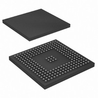
AT91SAM9XE512-CU Atmel, AT91SAM9XE512-CU Datasheet - Page 784

AT91SAM9XE512-CU
Manufacturer Part Number
AT91SAM9XE512-CU
Description
MCU ARM9 512K FLASH 217-BGA
Manufacturer
Atmel
Series
AT91SAMr
Datasheet
1.AT91SAM9XE128-QU.pdf
(860 pages)
Specifications of AT91SAM9XE512-CU
Core Processor
ARM9
Core Size
16/32-Bit
Speed
180MHz
Connectivity
EBI/EMI, Ethernet, I²C, MMC, SPI, SSC, UART/USART, USB
Peripherals
Brown-out Detect/Reset, POR, PWM, WDT
Number Of I /o
96
Program Memory Size
512KB (512K x 8)
Program Memory Type
FLASH
Ram Size
56K x 8
Voltage - Supply (vcc/vdd)
1.65 V ~ 1.95 V
Data Converters
A/D 4x10b
Oscillator Type
Internal
Operating Temperature
-40°C ~ 85°C
Package / Case
217-LFBGA
Package
217LFBGA
Device Core
ARM926EJ-S
Family Name
91S
Maximum Speed
180 MHz
Operating Supply Voltage
1.8|2.5|3.3 V
Data Bus Width
32 Bit
Number Of Programmable I/os
96
Interface Type
EBI/Ethernet/SPI/TWI/USART/USB
On-chip Adc
4-chx10-bit
Number Of Timers
6
Processor Series
AT91SAMx
Core
ARM926EJ-S
Data Ram Size
32 KB
Maximum Clock Frequency
180 MHz
Maximum Operating Temperature
+ 85 C
Mounting Style
SMD/SMT
3rd Party Development Tools
JTRACE-ARM-2M, KSK-AT91SAM9XE-PL, MDK-ARM, RL-ARM, ULINK2
Development Tools By Supplier
AT91SAM-ICE, AT91-ISP, AT91SAM9XE-EK
Minimum Operating Temperature
- 40 C
For Use With
AT91SAM9XE-EK - KIT EVAL FOR AT91SAM9XEAT91SAM-ICE - EMULATOR FOR AT91 ARM7/ARM9
Lead Free Status / RoHS Status
Lead free / RoHS Compliant
Eeprom Size
-
Lead Free Status / Rohs Status
Details
Available stocks
Company
Part Number
Manufacturer
Quantity
Price
Company:
Part Number:
AT91SAM9XE512-CU
Manufacturer:
NEC
Quantity:
201
Part Number:
AT91SAM9XE512-CU
Manufacturer:
ATMEL/爱特梅尔
Quantity:
20 000
- Current page: 784 of 860
- Download datasheet (13Mb)
42.5.5
42.5.6
784
AT91SAM9XE128/256/512 Preliminary
Conversion Triggers
Sleep Mode and Conversion Sequencer
Conversions of the active analog channels are started with a software or a hardware trigger. The
software trigger is provided by writing the Control Register (ADC_CR) with the bit START at 1.
The hardware trigger can be one of the TIOA outputs of the Timer Counter channels, or the
external trigger input of the ADC (ADTRG). The hardware trigger is selected with the field TRG-
SEL in the Mode Register (ADC_MR). The selected hardware trigger is enabled with the bit
TRGEN in the Mode Register (ADC_MR).
If a hardware trigger is selected, the start of a conversion is detected at each rising edge of the
selected signal. If one of the TIOA outputs is selected, the corresponding Timer Counter channel
must be programmed in Waveform Mode.
Only one start command is necessary to initiate a conversion sequence on all the channels. The
ADC hardware logic automatically performs the conversions on the active channels, then waits
for a new request. The Channel Enable (ADC_CHER) and Channel Disable (ADC_CHDR) Reg-
isters enable the analog channels to be enabled or disabled independently.
If the ADC is used with a PDC, only the transfers of converted data from enabled channels are
performed and the resulting data buffers should be interpreted accordingly.
Warning: Enabling hardware triggers does not disable the software trigger functionality. Thus, if
a hardware trigger is selected, the start of a conversion can be initiated either by the hardware or
the software trigger.
The ADC Sleep Mode maximizes power saving by automatically deactivating the ADC when it is
not being used for conversions. Sleep Mode is selected by setting the bit SLEEP in the Mode
Register ADC_MR.
The SLEEP mode is automatically managed by a conversion sequencer, which can automati-
cally process the conversions of all channels at lowest power consumption.
When a start conversion request occurs, the ADC is automatically activated. As the analog cell
requires a start-up time, the logic waits during this time and starts the conversion on the enabled
channels. When all conversions are complete, the ADC is deactivated until the next trigger. Trig-
gers occurring during the sequence are not taken into account.
The conversion sequencer allows automatic processing with minimum processor intervention
and optimized power consumption. Conversion sequences can be performed periodically using
a Timer/Counter output. The periodic acquisition of several samples can be processed automat-
ically without any intervention of the processor thanks to the PDC.
Note:
The reference voltage pins always remain connected in normal mode as in sleep mode.
6254C–ATARM–22-Jan-10
Related parts for AT91SAM9XE512-CU
Image
Part Number
Description
Manufacturer
Datasheet
Request
R

Part Number:
Description:
KIT EVAL FOR AT91SAM9XE
Manufacturer:
Atmel
Datasheet:

Part Number:
Description:
MCU ARM9 64K SRAM 144-LFBGA
Manufacturer:
Atmel
Datasheet:

Part Number:
Description:
IC ARM7 MCU FLASH 256K 100LQFP
Manufacturer:
Atmel
Datasheet:

Part Number:
Description:
IC ARM9 MPU 217-LFBGA
Manufacturer:
Atmel
Datasheet:

Part Number:
Description:
MCU ARM9 ULTRA LOW PWR 217-LFBGA
Manufacturer:
Atmel
Datasheet:

Part Number:
Description:
MCU ARM9 324-TFBGA
Manufacturer:
Atmel
Datasheet:

Part Number:
Description:
IC MCU ARM9 SAMPLING 217CBGA
Manufacturer:
Atmel
Datasheet:

Part Number:
Description:
IC ARM9 MCU 217-LFBGA
Manufacturer:
Atmel
Datasheet:

Part Number:
Description:
IC ARM9 MCU 208-PQFP
Manufacturer:
Atmel
Datasheet:

Part Number:
Description:
MCU ARM 512K HS FLASH 100-LQFP
Manufacturer:
Atmel
Datasheet:

Part Number:
Description:
MCU ARM 512K HS FLASH 100-TFBGA
Manufacturer:
Atmel
Datasheet:

Part Number:
Description:
IC ARM9 MCU 200 MHZ 324-TFBGA
Manufacturer:
Atmel
Datasheet:

Part Number:
Description:
IC ARM MCU 16BIT 128K 256BGA
Manufacturer:
Atmel
Datasheet:

Part Number:
Description:
IC ARM7 MCU 32BIT 128K 64LQFP
Manufacturer:
Atmel
Datasheet:

Part Number:
Description:
IC ARM7 MCU FLASH 256K 128-LQFP
Manufacturer:
Atmel
Datasheet:


