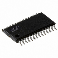
P89LPC9341FDH,512 NXP Semiconductors, P89LPC9341FDH,512 Datasheet - Page 29

P89LPC9341FDH,512
Manufacturer Part Number
P89LPC9341FDH,512
Description
IC 80C51 MCU FLASH 8K 28-TSSOP
Manufacturer
NXP Semiconductors
Series
LPC900r
Datasheet
1.P89LPC9351FA112.pdf
(94 pages)
Specifications of P89LPC9341FDH,512
Program Memory Type
FLASH
Program Memory Size
8KB (8K x 8)
Package / Case
28-TSSOP
Core Processor
8051
Core Size
8-Bit
Speed
18MHz
Connectivity
I²C, SPI, UART/USART
Peripherals
Brown-out Detect/Reset, POR, PWM, WDT
Number Of I /o
26
Ram Size
256 x 8
Voltage - Supply (vcc/vdd)
2.4 V ~ 3.6 V
Data Converters
A/D 8x8b; D/A 2x8b
Oscillator Type
Internal
Operating Temperature
-40°C ~ 85°C
Processor Series
P89LPC
Core
80C51
Data Bus Width
8 bit
Data Ram Size
256 B
Interface Type
I2C, SPI, UART
Maximum Clock Frequency
18 MHz
Number Of Programmable I/os
23
Number Of Timers
2
Operating Supply Voltage
2.4 V to 3.6 V
Maximum Operating Temperature
+ 85 C
Mounting Style
SMD/SMT
3rd Party Development Tools
PK51, CA51, A51, ULINK2
Minimum Operating Temperature
- 40 C
On-chip Adc
2 (8 bit, 4 Channel)
Lead Free Status / RoHS Status
Lead free / RoHS Compliant
For Use With
568-1758 - BOARD EVAL FOR LPC93X MCU FAMILY
Eeprom Size
-
Lead Free Status / Rohs Status
Lead free / RoHS Compliant
Other names
935288632512
Table 7.
[1]
[2]
[3]
[4]
Name
BODCFG
CLKCON
PGACON1
PGACON1B
PGA1TRIM8X16X PGA1 trim
PGA1TRIM2X4X
PGACON0
PGACON0B
PGA0TRIM8X16X PGA0 trim
PGA0TRIM2X4X
RTCDATH
RTCDATL
Extended SFRs are physically located on-chip but logically located in external data memory address space (XDATA). The MOVX A,@DPTR and MOVX @DPTR,A instructions are
used to access these extended SFRs.
The BOICFG1/0 will be copied from UCFG1.5 and UCFG1.3 when power-on reset.
CLKCON register reset value comes from UCFG1 and UCFG2. The reset value of CLKCON.2 to CLKCON.0 come from UCFG1.2 to UCFG1.0 and reset value of CLKDBL bit
comes from UCFG2.7.
On power-on reset and watchdog reset, the PGAxTRIM8X16X and PGAxTRIM2X4X registers are initialized with a factory preprogrammed value. Other resets will not cause
initialization.
Extended special function registers - P89LPC9351/9361
Description
BOD
configuration
register
CLOCK
Control
register
PGA1 control
register
PGA1 control
register B
register
PGA1 trim
register
PGA0 control
register
PGA0 control
register B
register
PGA0 trim
register
Real-time
clock data
register high
Real-time
clock data
register low
SFR
addr.
FFDEH
FFCAH
FFCEH
FFCDH 16XTRIM3 16XTRIM2 16XTRIM1 16XTRIM0 8XTRIM3
FFCCH
FFC8H
FFE1H
FFE4H
FFE3H 16XTRIM3 16XTRIM2 16XTRIM1 16XTRIM0 8XTRIM3
FFE2H
FFBFH
FFBEH
Bit functions and addresses
4XTRIM3
4XTRIM3
ENPGA1
ENPGA0
CLKOK
MSB
-
-
-
PGASEL1
PGASEL0
4XTRIM2
4XTRIM2
1
1
-
-
-
-
PGASEL1
PGASEL0
4XTRIM1
4XTRIM1
[1]
0
0
-
-
-
-
PGATRIM
PGATRIM
4XTRIM0
4XTRIM0
XTALWD
1
0
-
-
-
2XTRIM3
2XTRIM3
CLKDBL
TSEL1
-
-
-
-
8XTRIM2
2XTRIM2
8XTRIM2
2XTRIM2
FOSC2
TSEL0
-
-
-
-
BOICFG1
8XTRIM1
2XTRIM1
8XTRIM1
2XTRIM1
PGAG11
PGAG01
FOSC1
-
-
BOICFG0
PGAENO
PGAENO
8XTRIM0
2XTRIM0
8XTRIM0
2XTRIM0
PGAG10
PGAG00
FOSC0
LSB
FF1
FF0
Reset value
Hex Binary
[2]
[3]
00
00
[4]
[4]
00
00
[4]
[4]
00
00
1000 xxxx
0000 0000
0000 0000
0000 0000
0000 0000
0000 0000
0000 0000


