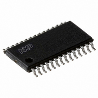
P89LPC9341FDH,512 NXP Semiconductors, P89LPC9341FDH,512 Datasheet - Page 76

P89LPC9341FDH,512
Manufacturer Part Number
P89LPC9341FDH,512
Description
IC 80C51 MCU FLASH 8K 28-TSSOP
Manufacturer
NXP Semiconductors
Series
LPC900r
Datasheet
1.P89LPC9351FA112.pdf
(94 pages)
Specifications of P89LPC9341FDH,512
Program Memory Type
FLASH
Program Memory Size
8KB (8K x 8)
Package / Case
28-TSSOP
Core Processor
8051
Core Size
8-Bit
Speed
18MHz
Connectivity
I²C, SPI, UART/USART
Peripherals
Brown-out Detect/Reset, POR, PWM, WDT
Number Of I /o
26
Ram Size
256 x 8
Voltage - Supply (vcc/vdd)
2.4 V ~ 3.6 V
Data Converters
A/D 8x8b; D/A 2x8b
Oscillator Type
Internal
Operating Temperature
-40°C ~ 85°C
Processor Series
P89LPC
Core
80C51
Data Bus Width
8 bit
Data Ram Size
256 B
Interface Type
I2C, SPI, UART
Maximum Clock Frequency
18 MHz
Number Of Programmable I/os
23
Number Of Timers
2
Operating Supply Voltage
2.4 V to 3.6 V
Maximum Operating Temperature
+ 85 C
Mounting Style
SMD/SMT
3rd Party Development Tools
PK51, CA51, A51, ULINK2
Minimum Operating Temperature
- 40 C
On-chip Adc
2 (8 bit, 4 Channel)
Lead Free Status / RoHS Status
Lead free / RoHS Compliant
For Use With
568-1758 - BOARD EVAL FOR LPC93X MCU FAMILY
Eeprom Size
-
Lead Free Status / Rohs Status
Lead free / RoHS Compliant
Other names
935288632512
NXP Semiconductors
11. Dynamic characteristics
Table 14.
V
T
P89LPC9331_9341_9351_9361
Product data sheet
Symbol
f
f
f
T
f
Glitch filter
t
t
External clock
t
t
t
t
Shift register (UART mode 0)
T
t
t
t
t
SPI interface
f
osc(RC)
osc(WD)
osc
CLKLP
gr
sa
CHCX
CLCX
CLCH
CHCL
QVXH
XHQX
XHDX
XHDV
SPI
amb
DD
cy(clk)
XLXL
= 2.4 V to 3.6 V unless otherwise specified.
=
−
40
°
Dynamic characteristics (12 MHz)
C to +85
Parameter
internal RC oscillator
frequency
internal watchdog
oscillator frequency
oscillator frequency
clock cycle time
low-power select clock
frequency
glitch rejection time
signal acceptance time
clock HIGH time
clock LOW time
clock rise time
clock fall time
serial port clock cycle
time
output data set-up to
clock rising edge time
output data hold after
clock rising edge time
input data hold after
clock rising edge time
input data valid to clock
rising edge time
SPI operating frequency
slave
master
°
C for industrial applications,
Conditions
nominal f = 7.3728 MHz
trimmed to ± 1 % at
T
doubler option = OFF
(default)
nominal f = 14.7456 MHz;
clock doubler option = ON,
V
T
see
P1.5/RST pin
any pin except P1.5/RST
P1.5/RST pin
any pin except P1.5/RST
see
see
see
see
see
see
see
see
see
amb
amb
DD
All information provided in this document is subject to legal disclaimers.
Figure 41
Figure 41
Figure 41
Figure 41
Figure 41
Figure 42
Figure 42
Figure 42
Figure 42
Figure 42
= 2.7 V to 3.6 V
= 25 °C; clock
= 25 °C
Rev. 5 — 10 January 2011
−
40
8-bit microcontroller with accelerated two-clock 80C51 core
°
C to +125
P89LPC9331/9341/9351/9361
°
C extended, unless otherwise specified.
16T
13T
14.378
7.189
Min
380
125
150
83
50
33
33
0
0
0
cy(clk)
cy(clk)
-
-
-
-
-
-
-
Variable clock
T
T
cy(clk)
T
cy(clk)
cy(clk)
15.114
CCLK
CCLK
7.557
Max
420
12
50
15
8
8
8
0
-
-
-
-
-
-
− t
− t
+ 20
⁄
⁄
6
4
CHCX
CLCX
14.378 15.114 MHz
7.189
f
1333
1083
osc
Min
380
125
150
50
33
33
0
-
-
-
-
-
-
-
-
-
-
© NXP B.V. 2011. All rights reserved.
= 12 MHz
[1][2]
7.557 MHz
Max
420
103
2.0
3.0
50
15
8
8
0
-
-
-
-
-
-
-
-
-
-
76 of 94
Unit
kHz
MHz
ns
MHz
ns
ns
ns
ns
ns
ns
ns
ns
ns
ns
ns
ns
ns
MHz
MHz


