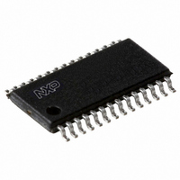
P89LPC9341FDH,512 NXP Semiconductors, P89LPC9341FDH,512 Datasheet - Page 42

P89LPC9341FDH,512
Manufacturer Part Number
P89LPC9341FDH,512
Description
IC 80C51 MCU FLASH 8K 28-TSSOP
Manufacturer
NXP Semiconductors
Series
LPC900r
Datasheet
1.P89LPC9351FA112.pdf
(94 pages)
Specifications of P89LPC9341FDH,512
Program Memory Type
FLASH
Program Memory Size
8KB (8K x 8)
Package / Case
28-TSSOP
Core Processor
8051
Core Size
8-Bit
Speed
18MHz
Connectivity
I²C, SPI, UART/USART
Peripherals
Brown-out Detect/Reset, POR, PWM, WDT
Number Of I /o
26
Ram Size
256 x 8
Voltage - Supply (vcc/vdd)
2.4 V ~ 3.6 V
Data Converters
A/D 8x8b; D/A 2x8b
Oscillator Type
Internal
Operating Temperature
-40°C ~ 85°C
Processor Series
P89LPC
Core
80C51
Data Bus Width
8 bit
Data Ram Size
256 B
Interface Type
I2C, SPI, UART
Maximum Clock Frequency
18 MHz
Number Of Programmable I/os
23
Number Of Timers
2
Operating Supply Voltage
2.4 V to 3.6 V
Maximum Operating Temperature
+ 85 C
Mounting Style
SMD/SMT
3rd Party Development Tools
PK51, CA51, A51, ULINK2
Minimum Operating Temperature
- 40 C
On-chip Adc
2 (8 bit, 4 Channel)
Lead Free Status / RoHS Status
Lead free / RoHS Compliant
For Use With
568-1758 - BOARD EVAL FOR LPC93X MCU FAMILY
Eeprom Size
-
Lead Free Status / Rohs Status
Lead free / RoHS Compliant
Other names
935288632512
NXP Semiconductors
P89LPC9331_9341_9351_9361
Product data sheet
7.22.4 Output compare
7.22.5 Input capture
7.22.6 PWM operation
When a reload occurs, the CCU Timer Overflow Interrupt Flag will be set, and an interrupt
generated if enabled. The 16-bit CCU timer may also be used as an 8-bit up/down timer.
There are four output compare channels: A, B, C and D. Each output compare channel
needs to be enabled in order to operate and the user will have to set the associated I/O
pin to the desired output mode to connect the pin. When the contents of the timer matches
that of a capture compare control register, the Timer Output Compare Interrupt Flag
(TOCFx) becomes set. An interrupt will occur if enabled.
Input capture is always enabled. Each time a capture event occurs on one of the two input
capture pins, the contents of the timer is transferred to the corresponding 16-bit input
capture register. The capture event can be programmed to be either rising or falling edge
triggered. A simple noise filter can be enabled on the input capture by enabling the Input
Capture Noise Filter bit. If set, the capture logic needs to see four consecutive samples of
the same value in order to recognize an edge as a capture event. An event counter can be
set to delay a capture by a number of capture events.
PWM operation has two main modes, symmetrical and asymmetrical.
In asymmetrical PWM operation the CCU timer operates in down-counting mode
regardless of the direction control bit.
In symmetrical mode, the timer counts up/down alternately. The main difference from
basic timer operation is the operation of the compare module, which in PWM mode is
used for PWM waveform generation.
As with basic timer operation, when the PWM (compare) pins are connected to the
compare logic, their logic state remains unchanged. However, since bit FCO is used to
hold the halt value, only a compare event can change the state of the pin.
Fig 9.
Asymmetrical PWM, down-counting
compare value
non-inverted
All information provided in this document is subject to legal disclaimers.
timer value
inverted
0x0000
TOR2
Rev. 5 — 10 January 2011
8-bit microcontroller with accelerated two-clock 80C51 core
P89LPC9331/9341/9351/9361
002aaa893
© NXP B.V. 2011. All rights reserved.
42 of 94


