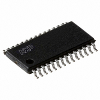
P89LPC9341FDH,512 NXP Semiconductors, P89LPC9341FDH,512 Datasheet - Page 8

P89LPC9341FDH,512
Manufacturer Part Number
P89LPC9341FDH,512
Description
IC 80C51 MCU FLASH 8K 28-TSSOP
Manufacturer
NXP Semiconductors
Series
LPC900r
Datasheet
1.P89LPC9351FA112.pdf
(94 pages)
Specifications of P89LPC9341FDH,512
Program Memory Type
FLASH
Program Memory Size
8KB (8K x 8)
Package / Case
28-TSSOP
Core Processor
8051
Core Size
8-Bit
Speed
18MHz
Connectivity
I²C, SPI, UART/USART
Peripherals
Brown-out Detect/Reset, POR, PWM, WDT
Number Of I /o
26
Ram Size
256 x 8
Voltage - Supply (vcc/vdd)
2.4 V ~ 3.6 V
Data Converters
A/D 8x8b; D/A 2x8b
Oscillator Type
Internal
Operating Temperature
-40°C ~ 85°C
Processor Series
P89LPC
Core
80C51
Data Bus Width
8 bit
Data Ram Size
256 B
Interface Type
I2C, SPI, UART
Maximum Clock Frequency
18 MHz
Number Of Programmable I/os
23
Number Of Timers
2
Operating Supply Voltage
2.4 V to 3.6 V
Maximum Operating Temperature
+ 85 C
Mounting Style
SMD/SMT
3rd Party Development Tools
PK51, CA51, A51, ULINK2
Minimum Operating Temperature
- 40 C
On-chip Adc
2 (8 bit, 4 Channel)
Lead Free Status / RoHS Status
Lead free / RoHS Compliant
For Use With
568-1758 - BOARD EVAL FOR LPC93X MCU FAMILY
Eeprom Size
-
Lead Free Status / Rohs Status
Lead free / RoHS Compliant
Other names
935288632512
NXP Semiconductors
Table 3.
P89LPC9331_9341_9351_9361
Product data sheet
Symbol
P0.0 to P0.7
P0.0/CMP2/
KBI0/AD01
P0.1/CIN2B/
KBI1/AD10
P0.2/CIN2A/
KBI2/AD11
P0.3/CIN1B/
KBI3/AD12
P0.4/CIN1A/
KBI4/DAC1/AD13
P0.5/CMPREF/
KBI5
Pin description
6.2 Pin description
Pin
PLCC28,
TSSOP28
3
26
25
24
23
22
Type Description
I/O
I/O
O
I
I
I/O
I
I
I
I/O
I
I
I
I/O
I
I
I
I/O
I
I
O
I
I/O
I
I
Port 0: Port 0 is an 8-bit I/O port with a user-configurable output type. During reset
Port 0 latches are configured in the input only mode with the internal pull-up
disabled. The operation of Port 0 pins as inputs and outputs depends upon the port
configuration selected. Each port pin is configured independently. Refer to
7.16.1 “Port configurations”
The Keypad Interrupt feature operates with Port 0 pins.
All pins have Schmitt trigger inputs.
Port 0 also provides various special functions as described below:
P0.0 — Port 0 bit 0.
CMP2 — Comparator 2 output
KBI0 — Keyboard input 0.
AD01 — ADC0 channel 1 analog input.
P0.1 — Port 0 bit 1.
CIN2B — Comparator 2 positive input B.
KBI1 — Keyboard input 1.
AD10 — ADC1 channel 0 analog input.
P0.2 — Port 0 bit 2.
CIN2A — Comparator 2 positive input A.
KBI2 — Keyboard input 2.
AD11 — ADC1 channel 1 analog input.
P0.3 — Port 0 bit 3. High current source.
CIN1B — Comparator 1 positive input B.
KBI3 — Keyboard input 3.
AD12 — ADC1 channel 2 analog input.
P0.4 — Port 0 bit 4. High current source.
CIN1A — Comparator 1 positive input A.
KBI4 — Keyboard input 4.
DAC1 — Digital-to-analog converter output 1.
AD13 — ADC1 channel 3 analog input.
P0.5 — Port 0 bit 5. High current source.
CMPREF — Comparator reference (negative) input.
KBI5 — Keyboard input 5.
All information provided in this document is subject to legal disclaimers.
Rev. 5 — 10 January 2011
8-bit microcontroller with accelerated two-clock 80C51 core
P89LPC9331/9341/9351/9361
and
Table 12 “Static characteristics”
© NXP B.V. 2011. All rights reserved.
for details.
Section
8 of 94


