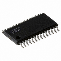
P89LPC9341FDH,512 NXP Semiconductors, P89LPC9341FDH,512 Datasheet - Page 30

P89LPC9341FDH,512
Manufacturer Part Number
P89LPC9341FDH,512
Description
IC 80C51 MCU FLASH 8K 28-TSSOP
Manufacturer
NXP Semiconductors
Series
LPC900r
Datasheet
1.P89LPC9351FA112.pdf
(94 pages)
Specifications of P89LPC9341FDH,512
Program Memory Type
FLASH
Program Memory Size
8KB (8K x 8)
Package / Case
28-TSSOP
Core Processor
8051
Core Size
8-Bit
Speed
18MHz
Connectivity
I²C, SPI, UART/USART
Peripherals
Brown-out Detect/Reset, POR, PWM, WDT
Number Of I /o
26
Ram Size
256 x 8
Voltage - Supply (vcc/vdd)
2.4 V ~ 3.6 V
Data Converters
A/D 8x8b; D/A 2x8b
Oscillator Type
Internal
Operating Temperature
-40°C ~ 85°C
Processor Series
P89LPC
Core
80C51
Data Bus Width
8 bit
Data Ram Size
256 B
Interface Type
I2C, SPI, UART
Maximum Clock Frequency
18 MHz
Number Of Programmable I/os
23
Number Of Timers
2
Operating Supply Voltage
2.4 V to 3.6 V
Maximum Operating Temperature
+ 85 C
Mounting Style
SMD/SMT
3rd Party Development Tools
PK51, CA51, A51, ULINK2
Minimum Operating Temperature
- 40 C
On-chip Adc
2 (8 bit, 4 Channel)
Lead Free Status / RoHS Status
Lead free / RoHS Compliant
For Use With
568-1758 - BOARD EVAL FOR LPC93X MCU FAMILY
Eeprom Size
-
Lead Free Status / Rohs Status
Lead free / RoHS Compliant
Other names
935288632512
NXP Semiconductors
P89LPC9331_9341_9351_9361
Product data sheet
7.3.1 Clock definitions
7.3.2 CPU clock (OSCCLK)
7.4.1 Low speed oscillator option
7.4.2 Medium speed oscillator option
7.4.3 High speed oscillator option
7.2 Enhanced CPU
7.3 Clocks
7.4 Crystal oscillator option
The P89LPC9331/9341/9351/9361 uses an enhanced 80C51 CPU which runs at
six times the speed of standard 80C51 devices. A machine cycle consists of two CPU
clock cycles, and most instructions execute in one or two machine cycles.
The P89LPC9331/9341/9351/9361 device has several internal clocks as defined below:
OSCCLK — Input to the DIVM clock divider. OSCCLK is selected from one of four clock
sources (see
Section 7.11 “CCLK modification: DIVM
Remark: f
CCLK — CPU clock; output of the clock divider. There are two CCLK cycles per machine
cycle, and most instructions are executed in one to two machine cycles (two or four CCLK
cycles).
RCCLK — The internal 7.373 MHz RC oscillator output. The clock doubler option, when
enabled, provides an output frequency of 14.746 MHz.
PCLK — Clock for the various peripheral devices and is
The P89LPC9331/9341/9351/9361 provides several user-selectable oscillator options in
generating the CPU clock. This allows optimization for a range of needs from high
precision to lowest possible cost. These options are configured when the flash is
programmed and include an on-chip watchdog oscillator, an on-chip RC oscillator, an
oscillator using an external crystal, or an external clock source.
The crystal oscillator option can be optimized for low, medium, or high frequency crystals
covering a range from 20 kHz to 18 MHz. It can be the clock source of OSCCLK, and
RTC. Low speed oscillator option can be the clock source of WDT.
This option supports an external crystal in the range of 20 kHz to 100 kHz. Ceramic
resonators are also supported in this configuration.
This option supports an external crystal in the range of 100 kHz to 4 MHz. Ceramic
resonators are also supported in this configuration.
This option supports an external crystal in the range of 4 MHz to 18 MHz. Ceramic
resonators are also supported in this configuration.
osc
Figure
is defined as the OSCCLK frequency.
All information provided in this document is subject to legal disclaimers.
7) and can also be optionally divided to a slower frequency (see
Rev. 5 — 10 January 2011
8-bit microcontroller with accelerated two-clock 80C51 core
P89LPC9331/9341/9351/9361
register”).
CCLK
⁄
2
.
© NXP B.V. 2011. All rights reserved.
30 of 94


