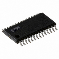
P89LPC9341FDH,512 NXP Semiconductors, P89LPC9341FDH,512 Datasheet - Page 67

P89LPC9341FDH,512
Manufacturer Part Number
P89LPC9341FDH,512
Description
IC 80C51 MCU FLASH 8K 28-TSSOP
Manufacturer
NXP Semiconductors
Series
LPC900r
Datasheet
1.P89LPC9351FA112.pdf
(94 pages)
Specifications of P89LPC9341FDH,512
Program Memory Type
FLASH
Program Memory Size
8KB (8K x 8)
Package / Case
28-TSSOP
Core Processor
8051
Core Size
8-Bit
Speed
18MHz
Connectivity
I²C, SPI, UART/USART
Peripherals
Brown-out Detect/Reset, POR, PWM, WDT
Number Of I /o
26
Ram Size
256 x 8
Voltage - Supply (vcc/vdd)
2.4 V ~ 3.6 V
Data Converters
A/D 8x8b; D/A 2x8b
Oscillator Type
Internal
Operating Temperature
-40°C ~ 85°C
Processor Series
P89LPC
Core
80C51
Data Bus Width
8 bit
Data Ram Size
256 B
Interface Type
I2C, SPI, UART
Maximum Clock Frequency
18 MHz
Number Of Programmable I/os
23
Number Of Timers
2
Operating Supply Voltage
2.4 V to 3.6 V
Maximum Operating Temperature
+ 85 C
Mounting Style
SMD/SMT
3rd Party Development Tools
PK51, CA51, A51, ULINK2
Minimum Operating Temperature
- 40 C
On-chip Adc
2 (8 bit, 4 Channel)
Lead Free Status / RoHS Status
Lead free / RoHS Compliant
For Use With
568-1758 - BOARD EVAL FOR LPC93X MCU FAMILY
Eeprom Size
-
Lead Free Status / Rohs Status
Lead free / RoHS Compliant
Other names
935288632512
NXP Semiconductors
Table 12.
V
T
[1]
[2]
[3]
[4]
[5]
[6]
[7]
[8]
[9]
[10] Measured with port in high-impedance mode.
[11] Port pins source a transition current when used in quasi-bidirectional mode and externally driven from logic 1 to logic 0. This current is
P89LPC9331_9341_9351_9361
Product data sheet
Symbol
I
I
I
R
V
TC
IL
LI
THL
amb
DD
ref(bg)
RST_N(int)
bg
= 2.4 V to 3.6 V unless otherwise specified.
Typical ratings are not guaranteed. The values listed are at room temperature, 3 V.
The I
The I
clock and watchdog timer.
The I
watchdog timer.
The I
brownout detect, and watchdog timer.
See
exceed the related specification.
This specification can be applied to pins which have A/D input or analog comparator input functions when the pin is not being used for
those analog functions. When the pin is being used as an analog input pin, the maximum voltage on the pin must be limited to 4.0 V with
respect to V
Pin capacitance is characterized but not tested.
Measured with port in quasi-bidirectional mode.
highest when V
=
−
40
Section 9 “Limiting values”
DD(idle)
DD(pd)
DD(oper)
DD(tpd)
°
Static characteristics
Parameter
LOW-level input current
input leakage current
HIGH-LOW transition
current
internal pull-up resistance
on pin RST
band gap reference voltage
band gap temperature
coefficient
C to +85
specification is measured using internal RC oscillator with the following functions disabled: comparators, real-time clock, and
specification is measured using an external clock with the following functions disabled: comparators, real-time clock,
specification is measured using an external clock with no active peripherals, with the following functions disabled: real-time
SS
specification is measured using an external clock with code while(1) {} executed from on-chip flash.
.
I
is approximately 2 V.
°
C for industrial applications,
for steady state (non-transient) limits on I
…continued
Conditions
V
V
all ports; V
V
pin RST
All information provided in this document is subject to legal disclaimers.
I
I
DD
= 0.4 V
= V
= 3.6 V
IL
, V
Rev. 5 — 10 January 2011
−
40
IH
I
8-bit microcontroller with accelerated two-clock 80C51 core
= 1.5 V at
, or V
°
C to +125
P89LPC9331/9341/9351/9361
th(HL)
°
C extended, unless otherwise specified.
OL
or I
[10]
[11]
OH
[9]
. If I
Min
-
-
−30
10
1.19
-
OL
/I
OH
exceeds the test condition, V
Typ
-
-
-
-
1.23
10
[1]
© NXP B.V. 2011. All rights reserved.
Max
−80
±1
−450
30
1.27
20
OL
/V
OH
Unit
μA
μA
μA
kΩ
V
ppm/
°C
67 of 94
may


