HD64F2612FA20 Renesas Electronics America, HD64F2612FA20 Datasheet - Page 159
HD64F2612FA20
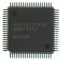
Manufacturer Part Number
HD64F2612FA20
Description
IC H8S MCU FLASH 128K 80QFP
Manufacturer
Renesas Electronics America
Series
H8® H8S/2600r
Specifications of HD64F2612FA20
Core Processor
H8S/2600
Core Size
16-Bit
Speed
20MHz
Connectivity
CAN, SCI
Peripherals
POR, PWM, WDT
Number Of I /o
43
Program Memory Size
128KB (128K x 8)
Program Memory Type
FLASH
Ram Size
4K x 8
Voltage - Supply (vcc/vdd)
4.5 V ~ 5.5 V
Data Converters
A/D 12x10b
Oscillator Type
Internal
Operating Temperature
-20°C ~ 75°C
Package / Case
80-QFP
Lead Free Status / RoHS Status
Contains lead / RoHS non-compliant
Eeprom Size
-
Available stocks
Company
Part Number
Manufacturer
Quantity
Price

Part Number:
HD64F2612FA20
Manufacturer:
RENESAS/瑞萨
Quantity:
20 000
Part Number:
HD64F2612FA20J
Manufacturer:
RENESAS/瑞萨
Quantity:
20 000


8.6
8.6.1
The procedure for using the DTC with interrupt activation is as follows:
1. Set the MRA, MRB, SAR, DAR, CRA, and CRB register information in on-chip RAM.
2. Set the start address of the register information in the DTC vector address.
3. Set the corresponding bit in DTCER to 1.
4. Set the enable bits for the interrupt sources to be used as the activation sources to 1. The DTC
5. After one data transfer has been completed, or after the specified number of data transfers have
8.6.2
The procedure for using the DTC with software activation is as follows:
1. Set the MRA, MRB, SAR, DAR, CRA, and CRB register information in on-chip RAM.
2. Set the start address of the register information in the DTC vector address.
3. Check that the SWDTE bit is 0.
4. Write 1 to SWDTE bit and the vector number to DTVECR.
5. Check the vector number written to DTVECR.
6. After one data transfer has been completed, if the DISEL bit is 0 and a CPU interrupt is not
8.7
8.7.1
An example is shown in which the DTC is used to receive 128 bytes of data via the SCI.
1. Set MRA to a fixed source address (SM1 = SM0 = 0), incrementing destination address (DM1
is activated when an interrupt used as an activation source is generated.
been completed, the DTCE bit is cleared to 0 and a CPU interrupt is requested. If the DTC is to
continue transferring data, set the DTCE bit to 1.
requested, the SWDTE bit is cleared to 0. If the DTC is to continue transferring data, set the
SWDTE bit to 1. When the DISEL bit is 1, or after the specified number of data transfers have
been completed, the SWDTE bit is held at 1 and a CPU interrupt is requested.
= 1, DM0 = 0), normal mode (MD1 = MD0 = 0), and byte size (Sz = 0). The DTS bit can have
any value. Set MRB for one data transfer by one interrupt (CHNE = 0, DISEL = 0). Set the
SCI RDR address in SAR, the start address of the RAM area where the data will be received in
DAR, and 128 (H'0080) in CRA. CRB can be set to any value.
Procedures for Using DTC
Activation by Interrupt
Activation by Software
Examples of Use of the DTC
Normal Mode
Rev. 7.00 Sep. 11, 2009 Page 123 of 566
Section 8 Data Transfer Controller (DTC)
REJ09B0211-0700
Related parts for HD64F2612FA20
Image
Part Number
Description
Manufacturer
Datasheet
Request
R


Part Number:
Description:
KIT STARTER FOR M16C/29
Manufacturer:
Renesas Electronics America
Datasheet:

Part Number:
Description:
KIT STARTER FOR R8C/2D
Manufacturer:
Renesas Electronics America
Datasheet:

Part Number:
Description:
R0K33062P STARTER KIT
Manufacturer:
Renesas Electronics America
Datasheet:

Part Number:
Description:
KIT STARTER FOR R8C/23 E8A
Manufacturer:
Renesas Electronics America
Datasheet:

Part Number:
Description:
KIT STARTER FOR R8C/25
Manufacturer:
Renesas Electronics America
Datasheet:

Part Number:
Description:
KIT STARTER H8S2456 SHARPE DSPLY
Manufacturer:
Renesas Electronics America
Datasheet:

Part Number:
Description:
KIT STARTER FOR R8C38C
Manufacturer:
Renesas Electronics America
Datasheet:

Part Number:
Description:
KIT STARTER FOR R8C35C
Manufacturer:
Renesas Electronics America
Datasheet:

Part Number:
Description:
KIT STARTER FOR R8CL3AC+LCD APPS
Manufacturer:
Renesas Electronics America
Datasheet:
Part Number:
Description:
KIT STARTER FOR RX610
Manufacturer:
Renesas Electronics America
Datasheet:

Part Number:
Description:
KIT STARTER FOR R32C/118
Manufacturer:
Renesas Electronics America
Datasheet:

Part Number:
Description:
KIT DEV RSK-R8C/26-29
Manufacturer:
Renesas Electronics America
Datasheet:

Part Number:
Description:
KIT STARTER FOR SH7124
Manufacturer:
Renesas Electronics America
Datasheet:

Part Number:
Description:
KIT STARTER FOR H8SX/1622
Manufacturer:
Renesas Electronics America
Datasheet: