HD64F2612FA20 Renesas Electronics America, HD64F2612FA20 Datasheet - Page 26
HD64F2612FA20
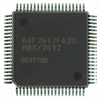
Manufacturer Part Number
HD64F2612FA20
Description
IC H8S MCU FLASH 128K 80QFP
Manufacturer
Renesas Electronics America
Series
H8® H8S/2600r
Specifications of HD64F2612FA20
Core Processor
H8S/2600
Core Size
16-Bit
Speed
20MHz
Connectivity
CAN, SCI
Peripherals
POR, PWM, WDT
Number Of I /o
43
Program Memory Size
128KB (128K x 8)
Program Memory Type
FLASH
Ram Size
4K x 8
Voltage - Supply (vcc/vdd)
4.5 V ~ 5.5 V
Data Converters
A/D 12x10b
Oscillator Type
Internal
Operating Temperature
-20°C ~ 75°C
Package / Case
80-QFP
Lead Free Status / RoHS Status
Contains lead / RoHS non-compliant
Eeprom Size
-
Available stocks
Company
Part Number
Manufacturer
Quantity
Price

Part Number:
HD64F2612FA20
Manufacturer:
RENESAS/瑞萨
Quantity:
20 000
Part Number:
HD64F2612FA20J
Manufacturer:
RENESAS/瑞萨
Quantity:
20 000


Figure 10.17 Cascaded Operation Setting Procedure .................................................................. 209
Figure 10.18 Example of Cascaded Operation (1)....................................................................... 210
Figure 10.19 Example of Cascaded Operation (2)....................................................................... 210
Figure 10.20 Example of PWM Mode Setting Procedure ........................................................... 213
Figure 10.21 Example of PWM Mode Operation (1) .................................................................. 214
Figure 10.22 Example of PWM Mode Operation (2) .................................................................. 214
Figure 10.23 Example of PWM Mode Operation (3) .................................................................. 215
Figure 10.24 Example of Phase Counting Mode Setting Procedure............................................ 217
Figure 10.25 Example of Phase Counting Mode 1 Operation ..................................................... 217
Figure 10.26 Example of Phase Counting Mode 2 Operation ..................................................... 218
Figure 10.27 Example of Phase Counting Mode 3 Operation ..................................................... 219
Figure 10.28 Example of Phase Counting Mode 4 Operation ..................................................... 220
Figure 10.29 Phase Counting Mode Application Example.......................................................... 222
Figure 10.30 Count Timing in Internal Clock Operation ............................................................ 226
Figure 10.31 Count Timing in External Clock Operation ........................................................... 226
Figure 10.32 Output Compare Output Timing ............................................................................ 227
Figure 10.33 Input Capture Input Signal Timing......................................................................... 227
Figure 10.34 Counter Clear Timing (Compare Match) ............................................................... 228
Figure 10.35 Counter Clear Timing (Input Capture) ................................................................... 228
Figure 10.36 Buffer Operation Timing (Compare Match) .......................................................... 229
Figure 10.37 Buffer Operation Timing (Input Capture) .............................................................. 229
Figure 10.38 TGI Interrupt Timing (Compare Match) ................................................................ 230
Figure 10.39 TGI Interrupt Timing (Input Capture).................................................................... 230
Figure 10.40 TCIV Interrupt Setting Timing............................................................................... 231
Figure 10.41 TCIU Interrupt Setting Timing............................................................................... 232
Figure 10.42 Timing for Status Flag Clearing by CPU ............................................................... 232
Figure 10.43 Timing for Status Flag Clearing by DTC Activation ............................................. 233
Figure 10.44 Phase Difference, Overlap, and Pulse Width in Phase Counting Mode ................. 234
Figure 10.45 Contention between TCNT Write and Clear Operations........................................ 235
Figure 10.46 Contention between TCNT Write and Increment Operations ................................ 236
Figure 10.47 Contention between TGR Write and Compare Match ........................................... 237
Figure 10.48 Contention between Buffer Register Write and Compare Match........................... 238
Figure 10.49 Contention between TGR Read and Input Capture ................................................ 239
Figure 10.50 Contention between TGR Write and Input Capture ............................................... 240
Figure 10.51 Contention between Buffer Register Write and Input Capture............................... 241
Figure 10.52 Contention between Overflow and Counter Clearing ............................................ 242
Figure 10.53 Contention between TCNT Write and Overflow ................................................... 243
Section 11 Motor Management Timer (MMT)
Figure 11.1
Figure 11.2
Rev. 7.00 Sep. 11, 2009 Page xxiv of xxxiv
REJ09B0211-0700
Block Diagram of MMT ........................................................................................ 246
Sample Operating Mode Setting Procedure ........................................................... 254
Related parts for HD64F2612FA20
Image
Part Number
Description
Manufacturer
Datasheet
Request
R


Part Number:
Description:
KIT STARTER FOR M16C/29
Manufacturer:
Renesas Electronics America
Datasheet:

Part Number:
Description:
KIT STARTER FOR R8C/2D
Manufacturer:
Renesas Electronics America
Datasheet:

Part Number:
Description:
R0K33062P STARTER KIT
Manufacturer:
Renesas Electronics America
Datasheet:

Part Number:
Description:
KIT STARTER FOR R8C/23 E8A
Manufacturer:
Renesas Electronics America
Datasheet:

Part Number:
Description:
KIT STARTER FOR R8C/25
Manufacturer:
Renesas Electronics America
Datasheet:

Part Number:
Description:
KIT STARTER H8S2456 SHARPE DSPLY
Manufacturer:
Renesas Electronics America
Datasheet:

Part Number:
Description:
KIT STARTER FOR R8C38C
Manufacturer:
Renesas Electronics America
Datasheet:

Part Number:
Description:
KIT STARTER FOR R8C35C
Manufacturer:
Renesas Electronics America
Datasheet:

Part Number:
Description:
KIT STARTER FOR R8CL3AC+LCD APPS
Manufacturer:
Renesas Electronics America
Datasheet:
Part Number:
Description:
KIT STARTER FOR RX610
Manufacturer:
Renesas Electronics America
Datasheet:

Part Number:
Description:
KIT STARTER FOR R32C/118
Manufacturer:
Renesas Electronics America
Datasheet:

Part Number:
Description:
KIT DEV RSK-R8C/26-29
Manufacturer:
Renesas Electronics America
Datasheet:

Part Number:
Description:
KIT STARTER FOR SH7124
Manufacturer:
Renesas Electronics America
Datasheet:

Part Number:
Description:
KIT STARTER FOR H8SX/1622
Manufacturer:
Renesas Electronics America
Datasheet: