HD64F2612FA20 Renesas Electronics America, HD64F2612FA20 Datasheet - Page 186
HD64F2612FA20
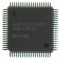
Manufacturer Part Number
HD64F2612FA20
Description
IC H8S MCU FLASH 128K 80QFP
Manufacturer
Renesas Electronics America
Series
H8® H8S/2600r
Specifications of HD64F2612FA20
Core Processor
H8S/2600
Core Size
16-Bit
Speed
20MHz
Connectivity
CAN, SCI
Peripherals
POR, PWM, WDT
Number Of I /o
43
Program Memory Size
128KB (128K x 8)
Program Memory Type
FLASH
Ram Size
4K x 8
Voltage - Supply (vcc/vdd)
4.5 V ~ 5.5 V
Data Converters
A/D 12x10b
Oscillator Type
Internal
Operating Temperature
-20°C ~ 75°C
Package / Case
80-QFP
Lead Free Status / RoHS Status
Contains lead / RoHS non-compliant
Eeprom Size
-
Available stocks
Company
Part Number
Manufacturer
Quantity
Price

Part Number:
HD64F2612FA20
Manufacturer:
RENESAS/瑞萨
Quantity:
20 000
Part Number:
HD64F2612FA20J
Manufacturer:
RENESAS/瑞萨
Quantity:
20 000


Section 9 I/O Ports
9.6.6
Port C pins also function as SCI_1 and SCI_0 I/O and interrupt input. The correspondence
between the register specification and the pin functions is shown below.
PC7: This pin function is switched as shown below.
PC6: This pin function is switched as shown below.
PC5/SCK1/IRQ5: The pin function is switched as shown below according to the operating mode,
bit C/A in the SCI1’s SMR, bits CKE0 and CKE1 in SCR, and bit PC5DDR.
PC4/RxD1: The pin function is switched as shown below according to the operating mode, bit RE
in the SCI1’s SCR, and bit PC4DDR.
Rev. 7.00 Sep. 11, 2009 Page 150 of 566
REJ09B0211-0700
PC7DDR
Pin function
PC6DDR
Pin function
CKE1
C/A
CKE0
PC5DDR
RE
PC4DDR
Pin function
Pin function
Pin Functions
IRQ5 input
PC5 input
0
PC4 input
0
0
PC5 output
0
1
0
PC7 input
PC6 input
0
0
0
SCK1 output
PC4 output
—
1
1
SCK1 output
—
—
1
PC7 output
PC6 output
RxD1 input
1
1
—
1
SCK1 input
—
—
—
1
Related parts for HD64F2612FA20
Image
Part Number
Description
Manufacturer
Datasheet
Request
R


Part Number:
Description:
KIT STARTER FOR M16C/29
Manufacturer:
Renesas Electronics America
Datasheet:

Part Number:
Description:
KIT STARTER FOR R8C/2D
Manufacturer:
Renesas Electronics America
Datasheet:

Part Number:
Description:
R0K33062P STARTER KIT
Manufacturer:
Renesas Electronics America
Datasheet:

Part Number:
Description:
KIT STARTER FOR R8C/23 E8A
Manufacturer:
Renesas Electronics America
Datasheet:

Part Number:
Description:
KIT STARTER FOR R8C/25
Manufacturer:
Renesas Electronics America
Datasheet:

Part Number:
Description:
KIT STARTER H8S2456 SHARPE DSPLY
Manufacturer:
Renesas Electronics America
Datasheet:

Part Number:
Description:
KIT STARTER FOR R8C38C
Manufacturer:
Renesas Electronics America
Datasheet:

Part Number:
Description:
KIT STARTER FOR R8C35C
Manufacturer:
Renesas Electronics America
Datasheet:

Part Number:
Description:
KIT STARTER FOR R8CL3AC+LCD APPS
Manufacturer:
Renesas Electronics America
Datasheet:
Part Number:
Description:
KIT STARTER FOR RX610
Manufacturer:
Renesas Electronics America
Datasheet:

Part Number:
Description:
KIT STARTER FOR R32C/118
Manufacturer:
Renesas Electronics America
Datasheet:

Part Number:
Description:
KIT DEV RSK-R8C/26-29
Manufacturer:
Renesas Electronics America
Datasheet:

Part Number:
Description:
KIT STARTER FOR SH7124
Manufacturer:
Renesas Electronics America
Datasheet:

Part Number:
Description:
KIT STARTER FOR H8SX/1622
Manufacturer:
Renesas Electronics America
Datasheet: