HD64F2612FA20 Renesas Electronics America, HD64F2612FA20 Datasheet - Page 22
HD64F2612FA20
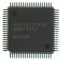
Manufacturer Part Number
HD64F2612FA20
Description
IC H8S MCU FLASH 128K 80QFP
Manufacturer
Renesas Electronics America
Series
H8® H8S/2600r
Specifications of HD64F2612FA20
Core Processor
H8S/2600
Core Size
16-Bit
Speed
20MHz
Connectivity
CAN, SCI
Peripherals
POR, PWM, WDT
Number Of I /o
43
Program Memory Size
128KB (128K x 8)
Program Memory Type
FLASH
Ram Size
4K x 8
Voltage - Supply (vcc/vdd)
4.5 V ~ 5.5 V
Data Converters
A/D 12x10b
Oscillator Type
Internal
Operating Temperature
-20°C ~ 75°C
Package / Case
80-QFP
Lead Free Status / RoHS Status
Contains lead / RoHS non-compliant
Eeprom Size
-
Available stocks
Company
Part Number
Manufacturer
Quantity
Price

Part Number:
HD64F2612FA20
Manufacturer:
RENESAS/瑞萨
Quantity:
20 000
Part Number:
HD64F2612FA20J
Manufacturer:
RENESAS/瑞萨
Quantity:
20 000


18.6 On-Board Programming Modes......................................................................................... 463
18.7 Flash Memory Emulation in RAM .................................................................................... 468
18.8 Flash Memory Programming/Erasing ................................................................................ 470
18.9 Program/Erase Protection .................................................................................................. 474
18.10 Programmer Mode ............................................................................................................. 475
18.11 Power-Down States for Flash Memory.............................................................................. 475
18.12 Note on Switching from F-ZTAT Version to Mask ROM Version ................................... 476
Section 19 Clock Pulse Generator .....................................................................477
19.1 Register Descriptions ......................................................................................................... 478
19.2 Oscillator............................................................................................................................ 480
19.3 PLL Circuit ........................................................................................................................ 483
19.4 Medium-Speed Clock Divider ........................................................................................... 483
19.5 Bus Master Clock Selection Circuit ................................................................................... 483
19.6 Usage Notes ....................................................................................................................... 484
Section 20 Power-Down Modes ........................................................................487
20.1 Register Descriptions ......................................................................................................... 490
20.2 Medium-Speed Mode......................................................................................................... 493
20.3 Sleep Mode ........................................................................................................................ 495
Rev. 7.00 Sep. 11, 2009 Page xx of xxxiv
REJ09B0211-0700
18.5.2 Flash Memory Control Register 2 (FLMCR2)...................................................... 461
18.5.3 Erase Block Register 1 (EBR1) ............................................................................ 461
18.5.4 Erase Block Register 2 (EBR2) ............................................................................ 462
18.5.5 RAM Emulation Register (RAMER).................................................................... 462
18.6.1 Boot Mode ............................................................................................................ 464
18.6.2 Programming/Erasing in User Program Mode...................................................... 466
18.8.1 Program/Program-Verify ...................................................................................... 470
18.8.2 Erase/Erase-Verify................................................................................................ 472
18.8.3 Interrupt Handling when Programming/Erasing Flash Memory........................... 472
18.9.1 Hardware Protection ............................................................................................. 474
18.9.2 Software Protection............................................................................................... 474
18.9.3 Error Protection..................................................................................................... 474
19.1.1 System Clock Control Register (SCKCR) ............................................................ 478
19.1.2 Low-Power Control Register (LPWRCR) ............................................................ 479
19.2.1 Connecting a Crystal Resonator............................................................................ 480
19.2.2 External Clock Input ............................................................................................. 481
19.6.1 Note on Crystal Resonator .................................................................................... 484
19.6.2 Note on Board Design........................................................................................... 484
20.1.1 Standby Control Register (SBYCR) ..................................................................... 490
20.1.2 Module Stop Control Registers A to C (MSTPCRA to MSTPCRC).................... 492
20.3.1 Transition to Sleep Mode...................................................................................... 495
Related parts for HD64F2612FA20
Image
Part Number
Description
Manufacturer
Datasheet
Request
R


Part Number:
Description:
KIT STARTER FOR M16C/29
Manufacturer:
Renesas Electronics America
Datasheet:

Part Number:
Description:
KIT STARTER FOR R8C/2D
Manufacturer:
Renesas Electronics America
Datasheet:

Part Number:
Description:
R0K33062P STARTER KIT
Manufacturer:
Renesas Electronics America
Datasheet:

Part Number:
Description:
KIT STARTER FOR R8C/23 E8A
Manufacturer:
Renesas Electronics America
Datasheet:

Part Number:
Description:
KIT STARTER FOR R8C/25
Manufacturer:
Renesas Electronics America
Datasheet:

Part Number:
Description:
KIT STARTER H8S2456 SHARPE DSPLY
Manufacturer:
Renesas Electronics America
Datasheet:

Part Number:
Description:
KIT STARTER FOR R8C38C
Manufacturer:
Renesas Electronics America
Datasheet:

Part Number:
Description:
KIT STARTER FOR R8C35C
Manufacturer:
Renesas Electronics America
Datasheet:

Part Number:
Description:
KIT STARTER FOR R8CL3AC+LCD APPS
Manufacturer:
Renesas Electronics America
Datasheet:
Part Number:
Description:
KIT STARTER FOR RX610
Manufacturer:
Renesas Electronics America
Datasheet:

Part Number:
Description:
KIT STARTER FOR R32C/118
Manufacturer:
Renesas Electronics America
Datasheet:

Part Number:
Description:
KIT DEV RSK-R8C/26-29
Manufacturer:
Renesas Electronics America
Datasheet:

Part Number:
Description:
KIT STARTER FOR SH7124
Manufacturer:
Renesas Electronics America
Datasheet:

Part Number:
Description:
KIT STARTER FOR H8SX/1622
Manufacturer:
Renesas Electronics America
Datasheet: