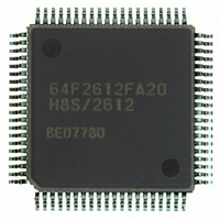
HD64F2612FA20 Renesas Electronics America, HD64F2612FA20 Datasheet - Page 294

HD64F2612FA20
Manufacturer Part Number
HD64F2612FA20
Description
IC H8S MCU FLASH 128K 80QFP
Manufacturer
Renesas Electronics America
Series
H8® H8S/2600r
Specifications of HD64F2612FA20
Core Processor
H8S/2600
Core Size
16-Bit
Speed
20MHz
Connectivity
CAN, SCI
Peripherals
POR, PWM, WDT
Number Of I /o
43
Program Memory Size
128KB (128K x 8)
Program Memory Type
FLASH
Ram Size
4K x 8
Voltage - Supply (vcc/vdd)
4.5 V ~ 5.5 V
Data Converters
A/D 12x10b
Oscillator Type
Internal
Operating Temperature
-20°C ~ 75°C
Package / Case
80-QFP
Lead Free Status / RoHS Status
Contains lead / RoHS non-compliant
Eeprom Size
-
Available stocks
Company
Part Number
Manufacturer
Quantity
Price
Part Number:
HD64F2612FA20
Manufacturer:
RENESAS/瑞萨
Quantity:
20 000
Part Number:
HD64F2612FA20J
Manufacturer:
RENESAS/瑞萨
Quantity:
20 000
- Current page: 294 of 606
- Download datasheet (4Mb)
Section 11 Motor Management Timer (MMT)
Set {PWM duty initial value – Td} in the free write operation addresses for TBRU to TBRW.
The values of TBRU to TBRW should always be set in the range H'0000 to H'FFFF – 2Td, and the
value of TPBR should always be set in the range H'0000 to H'FFFF – 4Td.
PWM Output Active Level Setting: In the operating modes, the active level of PWM pulses is
set with bits OLSN and OLSP in the timer mode register (TMDR).
The output level can be set for the three positive phases and the three negative phases of 6-phase
output. The operating mode must be exited before setting or changing the output level.
Dead Time Setting: In the operating modes, PWM pulses are output with a non-overlap
relationship between the positive and negative phases. This non-overlap time is known as the dead
time. The non-overlap time is set in the timer dead time data register (TDDR). The dead time
generation waveform is generated by comparing the value set in TDDR with the timer dead time
counters (TDCNT) for each phase. The operating mode must be exited before changing the
contents of TDDR.
PWM Period Setting: In the operating modes, 1/2 the PWM pulse period is set in the TPBR
register. The TPBR value should always be set in the range H'0000 to H'FFFF – 4Td. The value
set in TPBR is transferred to TPDR at the timing selected with bits MD1 and MD0 in the timer
mode register (TMDR). After the transfer, the value in TPDR is {TPBR value + 2Td}.
The new PWM period is effective from the next period when data is updated at the TCNT counter
crest, and from the same period when data is updated at the trough.
Register Updating: In the operating modes, buffer registers are used to update compare register
data. Update data can be written to a buffer register at all times. The buffer register value is
transferred to the compare register at the timing set by bits MD1 and MD0 in the timer mode
register (TMDR) (except in the case of a write to the free operation address for TBRU to TBRW,
in which case the value is transferred to the corresponding compare register immediately).
Initial Output in Operating Modes: The initial output in the operating modes is determined by
the initial values of TBRU to TBRW.
Table 11.2 shows the relationship between the initial value of TBRU to TBRW and the initial
output.
Rev. 7.00 Sep. 11, 2009 Page 258 of 566
REJ09B0211-0700
Related parts for HD64F2612FA20
Image
Part Number
Description
Manufacturer
Datasheet
Request
R

Part Number:
Description:
KIT STARTER FOR M16C/29
Manufacturer:
Renesas Electronics America
Datasheet:

Part Number:
Description:
KIT STARTER FOR R8C/2D
Manufacturer:
Renesas Electronics America
Datasheet:

Part Number:
Description:
R0K33062P STARTER KIT
Manufacturer:
Renesas Electronics America
Datasheet:

Part Number:
Description:
KIT STARTER FOR R8C/23 E8A
Manufacturer:
Renesas Electronics America
Datasheet:

Part Number:
Description:
KIT STARTER FOR R8C/25
Manufacturer:
Renesas Electronics America
Datasheet:

Part Number:
Description:
KIT STARTER H8S2456 SHARPE DSPLY
Manufacturer:
Renesas Electronics America
Datasheet:

Part Number:
Description:
KIT STARTER FOR R8C38C
Manufacturer:
Renesas Electronics America
Datasheet:

Part Number:
Description:
KIT STARTER FOR R8C35C
Manufacturer:
Renesas Electronics America
Datasheet:

Part Number:
Description:
KIT STARTER FOR R8CL3AC+LCD APPS
Manufacturer:
Renesas Electronics America
Datasheet:

Part Number:
Description:
KIT STARTER FOR RX610
Manufacturer:
Renesas Electronics America
Datasheet:

Part Number:
Description:
KIT STARTER FOR R32C/118
Manufacturer:
Renesas Electronics America
Datasheet:

Part Number:
Description:
KIT DEV RSK-R8C/26-29
Manufacturer:
Renesas Electronics America
Datasheet:

Part Number:
Description:
KIT STARTER FOR SH7124
Manufacturer:
Renesas Electronics America
Datasheet:

Part Number:
Description:
KIT STARTER FOR H8SX/1622
Manufacturer:
Renesas Electronics America
Datasheet:


