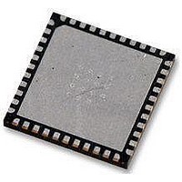
AT89LP52-20MU Atmel, AT89LP52-20MU Datasheet - Page 16

AT89LP52-20MU
Manufacturer Part Number
AT89LP52-20MU
Description
IC MCU 8051 8K FLASH SPI 44VQFN
Manufacturer
Atmel
Series
89LPr
Datasheet
1.AT89LP52-20MU.pdf
(113 pages)
Specifications of AT89LP52-20MU
Core Processor
8051
Core Size
8-Bit
Speed
20MHz
Connectivity
EBI/EMI, I²C, SPI, UART/USART
Peripherals
Brown-out Detect/Reset, POR, PWM, WDT
Number Of I /o
36
Program Memory Size
8KB (8K x 8)
Program Memory Type
FLASH
Ram Size
256 x 8
Voltage - Supply (vcc/vdd)
2.4 V ~ 5.5 V
Oscillator Type
Internal
Operating Temperature
-40°C ~ 85°C
Package / Case
44-VFQFN Exposed Pad
Processor Series
AT89x
Core
8051
Data Bus Width
8 bit
Data Ram Size
256 B
Interface Type
Serial
Maximum Clock Frequency
20 MHz
Number Of Programmable I/os
36
Number Of Timers
3
Operating Supply Voltage
2.7 V to 5.5 V
Maximum Operating Temperature
+ 85 C
Mounting Style
SMD/SMT
Lead Free Status / RoHS Status
Lead free / RoHS Compliant
Eeprom Size
-
Data Converters
-
Lead Free Status / Rohs Status
Details
Available stocks
Company
Part Number
Manufacturer
Quantity
Price
Company:
Part Number:
AT89LP52-20MU
Manufacturer:
Atmel
Quantity:
490
16
AT89LP51/52 - Preliminary
Figure 3-8.
Figure 3-9.
The auto-erase bit AERS (MEMCON.6) can be set to one to perform a page erase automatically
at the beginning of any write sequence. The page erase will erase the entire page, i.e. both the
low and high half pages. However, the write operation paired with the auto-erase can only pro-
gram one of the half pages. A second write cycle without auto-erase is required to update the
other half page.
Frequently just a few bytes within a page must be updated while maintaining the state of the
other bytes. There are two options for handling this situation that allow the Flash Data memory
to emulate a traditional EEPROM memory. The simplest method is to copy the entire page into a
buffer allocated in RAM, modify the desired byte locations in the RAM buffer, and then load and
write back first the low half page (with auto-erase) and then the high half page to the Flash mem-
ory. This option requires that at least one page size of RAM is available as a temporary buffer.
The second option is to store only one half page in RAM. The unmodified bytes of the other page
are loaded directly into the Flash memory’s temporary load buffer before loading the updated
values of the modified bytes. For example, if just the low half page needs modification, the user
must first store the high half page to RAM, followed by reading and loading the unaffected bytes
of the low half page into the page buffer. Then the modified bytes of the low half page are stored
to the page buffer before starting the auto-erase sequence. The stored value of the high half
page must be written without auto-erase after the programming of the low half page completes.
This method reduces the amount of RAM required; however, more software overhead is needed
because the read-and-load-back routine must skip those bytes in the page that need to be
updated in order to prevent those locations in the buffer from being loaded with the previous
data, as this will block the new data from being loaded correctly.
A write sequence will not occur if the Brown-out Detector is active. If a write currently in progress
is interrupted by the BOD due to a low voltage condition, the ERR flag will be set.
MWEN
MWEN
DMEN
MOVX
DMEN
MOVX
LDPG
LDPG
FDATA Byte Write
IDLE
FDATA Page Write
IDLE
t
WC
t
WC
t
WC
3709B–MICRO–12/10


