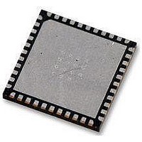
AT89LP52-20MU Atmel, AT89LP52-20MU Datasheet - Page 92

AT89LP52-20MU
Manufacturer Part Number
AT89LP52-20MU
Description
IC MCU 8051 8K FLASH SPI 44VQFN
Manufacturer
Atmel
Series
89LPr
Datasheet
1.AT89LP52-20MU.pdf
(113 pages)
Specifications of AT89LP52-20MU
Core Processor
8051
Core Size
8-Bit
Speed
20MHz
Connectivity
EBI/EMI, I²C, SPI, UART/USART
Peripherals
Brown-out Detect/Reset, POR, PWM, WDT
Number Of I /o
36
Program Memory Size
8KB (8K x 8)
Program Memory Type
FLASH
Ram Size
256 x 8
Voltage - Supply (vcc/vdd)
2.4 V ~ 5.5 V
Oscillator Type
Internal
Operating Temperature
-40°C ~ 85°C
Package / Case
44-VFQFN Exposed Pad
Processor Series
AT89x
Core
8051
Data Bus Width
8 bit
Data Ram Size
256 B
Interface Type
Serial
Maximum Clock Frequency
20 MHz
Number Of Programmable I/os
36
Number Of Timers
3
Operating Supply Voltage
2.7 V to 5.5 V
Maximum Operating Temperature
+ 85 C
Mounting Style
SMD/SMT
Lead Free Status / RoHS Status
Lead free / RoHS Compliant
Eeprom Size
-
Data Converters
-
Lead Free Status / Rohs Status
Details
Available stocks
Company
Part Number
Manufacturer
Quantity
Price
Company:
Part Number:
AT89LP52-20MU
Manufacturer:
Atmel
Quantity:
490
18. Electrical Characteristics
18.1
18.2
T
Notes:
92
Operating Temperature ................................... -40°C to +85°C
Storage Temperature ..................................... -65°C to +150°C
Voltage on Any Pin with Respect to Ground......-0.7V to +5.5V
Maximum Operating Voltage ............................................ 5.5V
Total DC Output Current ........................................... 150.0 mA
A
Symbol
V
V
V
V
V
I
I
I
R
C
I
IL
TL
LI
CC
OL
OH
OH1
IL
IH
RST
IO
= -40°C to 85°C, V
Absolute Maximum Ratings*
DC Characteristics
1. Under steady state (non-transient) conditions, I
2. Minimum V
3. All characteristics contained in this datasheet are based on simulation and characterization of other microcontrollers manu-
AT89LP51/52 - Preliminary
Maximum I
Maximum total I
If I
than the listed test conditions.
factured in the same process technology. These values are preliminary values representing design targets, and will be
updated after characterization of actual silicon.
OL
Parameter
Input Low-voltage
Input High-voltage
Output Low-voltage
Output High-voltage
With Weak Pull-ups Enabled
Output High-voltage
With Strong Pull-ups Enabled
Logic 0 Input Current
Logic 1 to 0 Transition Current
Input Leakage Current
Reset Pull-up Resistor
Pin Capacitance
Power Supply Current
(Fast Mode)
Power Supply Current
(Compatibility Mode)
Power-down Mode
exceeds the test condition, V
OL
DD
DD
per port pin: 10 mA
for Power-down is 2V.
= 2.4V to 5.5V (unless otherwise noted)
OL
for all output pins: 100 mA
(2)
(1)
OL
may exceed the related specification. Pins are not guaranteed to sink current greater
Condition
I
I
I
I
I
I
V
V
0 < V
Test Freq. = 1 MHz, T
Active Mode, 12 MHz, V
Idle Mode, 12 MHz, V
Active Mode, 12 MHz, V
Idle Mode, 12 MHz, V
V
V
OL
OH
OH
OH
OH
OH
IN
IN
DD
DD
= 10 mA, V
= -80 µA, V
= -30 µA
= -12 µA
= -10 mA, T
= -5 mA, T
= 0.45V
= 2V, V
= 5.5V
= 3V
IN
< V
OL
DD
DD
must be externally limited as follows:
= 5V ± 10%
A
DD
DD
A
= 85°C
= 85°C
= 2.4V, T
= 3V ± 10%
*NOTICE:
A
DD
DD
= 25°C
DD
DD
= 5.5V
= 5.5V
A
= 5.5V
= 5.5V
= 85°C
Stresses beyond those listed under “Absolute
Maximum Ratings” may cause permanent dam-
age to the device. This is a stress rating only and
functional operation of the device at these or any
other conditions beyond those indicated in the
operational sections of this specification is not
implied. Exposure to absolute maximum rating
conditions for extended periods may affect
device reliability.
0.2 V
0.75 V
0.75 V
0.9 V
0.9 V
Min
-0.5
2.4
DD
50
+ 0.9
DD
DD
DD
DD
0.2 V
V
DD
Max
-750
150
±10
0.5
-50
10
DD
7
3
5
3
5
2
+ 0.5
3709B–MICRO–12/10
- 0.1
Units
mA
mA
mA
mA
µA
µA
µA
pF
µA
µA
kΩ
V
V
V
V
V
V


