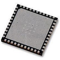
AT89LP52-20MU Atmel, AT89LP52-20MU Datasheet - Page 6

AT89LP52-20MU
Manufacturer Part Number
AT89LP52-20MU
Description
IC MCU 8051 8K FLASH SPI 44VQFN
Manufacturer
Atmel
Series
89LPr
Datasheet
1.AT89LP52-20MU.pdf
(113 pages)
Specifications of AT89LP52-20MU
Core Processor
8051
Core Size
8-Bit
Speed
20MHz
Connectivity
EBI/EMI, I²C, SPI, UART/USART
Peripherals
Brown-out Detect/Reset, POR, PWM, WDT
Number Of I /o
36
Program Memory Size
8KB (8K x 8)
Program Memory Type
FLASH
Ram Size
256 x 8
Voltage - Supply (vcc/vdd)
2.4 V ~ 5.5 V
Oscillator Type
Internal
Operating Temperature
-40°C ~ 85°C
Package / Case
44-VFQFN Exposed Pad
Processor Series
AT89x
Core
8051
Data Bus Width
8 bit
Data Ram Size
256 B
Interface Type
Serial
Maximum Clock Frequency
20 MHz
Number Of Programmable I/os
36
Number Of Timers
3
Operating Supply Voltage
2.7 V to 5.5 V
Maximum Operating Temperature
+ 85 C
Mounting Style
SMD/SMT
Lead Free Status / RoHS Status
Lead free / RoHS Compliant
Eeprom Size
-
Data Converters
-
Lead Free Status / Rohs Status
Details
Available stocks
Company
Part Number
Manufacturer
Quantity
Price
Company:
Part Number:
AT89LP52-20MU
Manufacturer:
Atmel
Quantity:
490
2. Overview
The AT89LP51/52 is a low-power, high-performance CMOS 8-bit microcontroller with 4K/8K
bytes of In-System Programmable Flash program memory and 256 bytes of Flash data memory.
The device is manufactured using Atmel's high-density nonvolatile memory technology and is
compatible with the industry-standard 80C52 instruction set.
The AT89LP51/52 is built around an enhanced CPU core that can fetch a single byte from mem-
ory every clock cycle. In the classic 8051 architecture, each fetch requires 6 clock cycles, forcing
instructions to execute in 12, 24 or 48 clock cycles. In the AT89LP51/52 CPU, instructions need
only 1 to 4 clock cycles providing 6 to 12 times more throughput than the standard 8051. Sev-
enty percent of instructions need only as many clock cycles as they have bytes to execute, and
most of the remaining instructions require only one additional clock. The enhanced CPU core is
capable of 20 MIPS throughput whereas the classic 8051 CPU can deliver only 4 MIPS at the
same current consumption. Conversely, at the same throughput as the classic 8051, the new
CPU core runs at a much lower speed and thereby greatly reducing power consumption and
EMI. The AT89LP51/52 also includes a compatibility mode that will enable classic 12 clock per
machine cycle operation for true timing compatibility with AT89S51/52.
The AT89LP51/52 provides the following standard features: 4K/8K bytes of In-System
Programmable Flash program memory, 256 bytes of Flash data memory, 256 bytes of RAM, up
to 36 I/O lines, three 16-bit timer/counters, a programmable watchdog timer, a full-duplex serial
port, an on-chip crystal oscillator, an internal 1.8432 MHz auxiliary oscillator, and a four-level,
six-vector interrupt system. A block diagram is shown in
Figure
2-1.
All three timer/counters of the AT89LP51/52, Timer 0, Timer 1 and Timer 2, can be configured to
toggle a port pin on overflow for clock/waveform generation. Unlike AT89S51, Timer 2 is also
present on AT89LP51.
The enhanced full-duplex UART of the AT89LP51/52 includes Framing Error Detection and
Automatic Address Recognition. In addition, enhancements to Mode 0 allow hardware acceler-
ated emulation of a Serial Peripheral Interface (SPI) or a Two-Wire Interface (TWI).
The Watchdog Timer of the AT89LP51/52 includes a 7-bit prescaler, a software reset command
and an overflow flag. The watchdog can be configured to output a reset pulse on the external
Reset pin.
Each 8-bit I/O port of the AT89LP51/52 can be independently configured in one of four operating
modes. In quasi-bidirectional mode, the port operates as in the classic 8051. In input-only mode,
the port is tristated. Push-pull output mode provides full CMOS drivers and open-drain mode
provides just a pull-down. Unlike other 8051s, this allows Port 0 to operate with on-chip pull-ups
if desired.
AT89LP51/52 - Preliminary
6
3709B–MICRO–12/10


