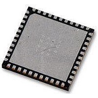
AT89LP52-20MU Atmel, AT89LP52-20MU Datasheet - Page 62

AT89LP52-20MU
Manufacturer Part Number
AT89LP52-20MU
Description
IC MCU 8051 8K FLASH SPI 44VQFN
Manufacturer
Atmel
Series
89LPr
Datasheet
1.AT89LP52-20MU.pdf
(113 pages)
Specifications of AT89LP52-20MU
Core Processor
8051
Core Size
8-Bit
Speed
20MHz
Connectivity
EBI/EMI, I²C, SPI, UART/USART
Peripherals
Brown-out Detect/Reset, POR, PWM, WDT
Number Of I /o
36
Program Memory Size
8KB (8K x 8)
Program Memory Type
FLASH
Ram Size
256 x 8
Voltage - Supply (vcc/vdd)
2.4 V ~ 5.5 V
Oscillator Type
Internal
Operating Temperature
-40°C ~ 85°C
Package / Case
44-VFQFN Exposed Pad
Processor Series
AT89x
Core
8051
Data Bus Width
8 bit
Data Ram Size
256 B
Interface Type
Serial
Maximum Clock Frequency
20 MHz
Number Of Programmable I/os
36
Number Of Timers
3
Operating Supply Voltage
2.7 V to 5.5 V
Maximum Operating Temperature
+ 85 C
Mounting Style
SMD/SMT
Lead Free Status / RoHS Status
Lead free / RoHS Compliant
Eeprom Size
-
Data Converters
-
Lead Free Status / Rohs Status
Details
Available stocks
Company
Part Number
Manufacturer
Quantity
Price
Company:
Part Number:
AT89LP52-20MU
Manufacturer:
Atmel
Quantity:
490
14.5
14.5.1
62
More About Mode 0
AT89LP51/52 - Preliminary
Two-Wire (Half-Duplex) Mode
The Broadcast Address for each slave is created by taking the logic OR of SADDR and SADEN.
Zeros in this result are trended as don’t cares. In most cases, interpreting the don’t cares as
ones, the broadcast address will be FF hexadecimal.
Upon reset SADDR (SFR address 0A9H) and SADEN (SFR address 0B9H) are loaded with
“0”s. This produces a given address of all “don’t cares” as well as a Broadcast address of all
“don’t cares”. This effectively disables the Automatic Addressing mode and allows the microcon-
troller to use standard 80C51-type UART drivers which do not make use of this feature.
In Mode 0, the UART is configured as either a two wire half-duplex or three wire full-duplex syn-
chronous serial interface. In two-wire mode serial data enters and exits through RXD and TXD
outputs the shift clock. In three-wire mode serial data enters through MISO, exits through MOSI
and SCK outputs the shift clock. Eight data bits are transmitted/received, with the LSB first.
ure 14-3
Mode 0 and associated timing. The baud rate is programmable to 1/2 or 1/4 the system fre-
quency by setting/clearing the SMOD1 bit in Fast mode, or 1/3 or 1/6 the system frequency in
Compatibility mode. However, changing SMOD1 has an effect on the relationship between the
clock and data as described below. The baud rate can also be generated by Timer 1 by setting
TB8.
Table 14-4.
Transmission is initiated by any instruction that uses SBUF as a destination register. The “write
to SBUF” signal also loads a “1” into the 9th position of the transmit shift register and tells the TX
Control Block to begin a transmission. The internal timing is such that one full bit slot may elapse
between “write to SBUF” and activation of SEND.
SEND transfers the output of the shift register to the alternate output function line of P3.0, and
also transfers Shift Clock to the alternate output function line of P3.1. As data bits shift out to the
right, “0”s come in from the left. When the MSB of the data byte is at the output position of the
shift register, the “1” that was initially loaded into the 9th position is just to the left of the MSB,
and all positions to the left of that contain “0”s. This condition flags the TX Control block to do
one last shift, then deactivate SEND and set TI.
Reception is initiated by the condition REN = 1 and RI = 0. At the next clock cycle, the RX Con-
trol unit writes the bits 11111110B to the receive shift register and activates RECEIVE in the
next clock phase. RECEIVE enables Shift Clock to the alternate output function line of P3.1. As
data bits come in from the right, “1”s shift out to the left. When the “0” that was initially loaded
into the right-most position arrives at the left-most position in the shift register, it flags the RX
Control block to do one last shift and load SBUF. Then RECEIVE is cleared and RI is set.
The relationship between the shift clock and data is determined by the combination of the SM2
and SMOD1 bits as listed in
TB8
0
0
1
1
Table 14-4
and
SMOD1
Figure 14-5 on page 67
Mode 0 Baud Rates
0
1
0
1
lists the baud rate options for Mode 0.
(Timer 1 Overflow) / 4
(Timer 1 Overflow) / 2
Baud Rate (Fast)
Table 14-5
f
f
SYS
SYS
/4
/2
show simplified functional diagrams of the serial port in
and shown in
Figure
Baud Rate (Compatibility)
(Timer 1 Overflow) / 4
(Timer 1 Overflow) / 2
. The SM2 bit determines the idle
f
f
SYS
SYS
/6
/3
3709B–MICRO–12/10
Fig-


