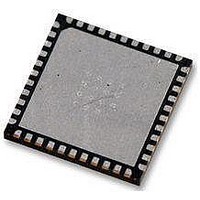
AT89LP52-20MU Atmel, AT89LP52-20MU Datasheet - Page 18

AT89LP52-20MU
Manufacturer Part Number
AT89LP52-20MU
Description
IC MCU 8051 8K FLASH SPI 44VQFN
Manufacturer
Atmel
Series
89LPr
Datasheet
1.AT89LP52-20MU.pdf
(113 pages)
Specifications of AT89LP52-20MU
Core Processor
8051
Core Size
8-Bit
Speed
20MHz
Connectivity
EBI/EMI, I²C, SPI, UART/USART
Peripherals
Brown-out Detect/Reset, POR, PWM, WDT
Number Of I /o
36
Program Memory Size
8KB (8K x 8)
Program Memory Type
FLASH
Ram Size
256 x 8
Voltage - Supply (vcc/vdd)
2.4 V ~ 5.5 V
Oscillator Type
Internal
Operating Temperature
-40°C ~ 85°C
Package / Case
44-VFQFN Exposed Pad
Processor Series
AT89x
Core
8051
Data Bus Width
8 bit
Data Ram Size
256 B
Interface Type
Serial
Maximum Clock Frequency
20 MHz
Number Of Programmable I/os
36
Number Of Timers
3
Operating Supply Voltage
2.7 V to 5.5 V
Maximum Operating Temperature
+ 85 C
Mounting Style
SMD/SMT
Lead Free Status / RoHS Status
Lead free / RoHS Compliant
Eeprom Size
-
Data Converters
-
Lead Free Status / Rohs Status
Details
Available stocks
Company
Part Number
Manufacturer
Quantity
Price
Company:
Part Number:
AT89LP52-20MU
Manufacturer:
Atmel
Quantity:
490
18
AT89LP51/52 - Preliminary
Figure 3-10. External Data Memory 16-bit Linear Address Mode
Figure 3-11
using an 8-bit paged address. Port 0 serves as a multiplexed address/data bus to the RAM. The
ALE strobe is used to latch the address byte into an external register so that Port 0 can be freed
for data input/output. The Port 2 I/O lines (or other ports) can provide control lines to page the
memory; however, this operation is not handled automatically by hardware. The software appli-
cation must change the Port 2 register when appropriate to access different pages. The
MOVX @Ri instructions use Paged Address mode.
Figure 3-11. External Data Memory 8-bit Paged Address Mode
Note that prior to using the external memory interface, WR (P3.6) and RD (P3.7) must be config-
ured as outputs. See
automatically to push-pull output mode when outputting address or data and P0 is automatically
tristated when inputting data regardless of the port configuration. The Port 0 configuration will
determine the idle state of Port 0 when not accessing the external memory.
Figure 3-12
respectively. The address on P0 and P2 is stable at the falling edge of ALE. The idle state of
ALE is controlled by DISALE (AUXR.0). When DISALE = 0 the ALE toggles at a constant rate
when not accessing external memory. When DISALE = 1 the ALE is weakly pulled high. DISALE
must be one in order to use P4.4 as a general-purpose I/O. The WS bits in AUXR can extended
the RD and WR strobes by 1, 2 or 3 cycles as shown in Figures 3-16, 3-17 and 3-18. If a longer
strobe is required, the application can scale the system clock with the clock divider to meet the
requirements (See
and
shows a hardware configuration for accessing 256-byte blocks of external RAM
Figure 3-13
Section 6.4 on page
Section 10.1 “Port Configuration” on page
P1
P1
RD
WR
RD
WR
show examples of external data memory write and read cycles,
AT89LP
AT89LP
P3
P3
P2
ALE
ALE
P0
P2
P0
30).
I/O
LATCH
LATCH
PAGE
BITS
DATA
DATA
EXTERNAL
EXTERNAL
WE
MEMORY
MEMORY
WE
ADDR
ADDR
DATA
DATA
40. P0 and P2 are configured
OE
OE
3709B–MICRO–12/10


