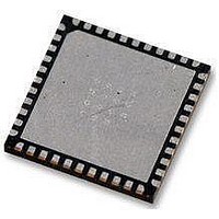
AT89LP52-20MU Atmel, AT89LP52-20MU Datasheet - Page 43

AT89LP52-20MU
Manufacturer Part Number
AT89LP52-20MU
Description
IC MCU 8051 8K FLASH SPI 44VQFN
Manufacturer
Atmel
Series
89LPr
Datasheet
1.AT89LP52-20MU.pdf
(113 pages)
Specifications of AT89LP52-20MU
Core Processor
8051
Core Size
8-Bit
Speed
20MHz
Connectivity
EBI/EMI, I²C, SPI, UART/USART
Peripherals
Brown-out Detect/Reset, POR, PWM, WDT
Number Of I /o
36
Program Memory Size
8KB (8K x 8)
Program Memory Type
FLASH
Ram Size
256 x 8
Voltage - Supply (vcc/vdd)
2.4 V ~ 5.5 V
Oscillator Type
Internal
Operating Temperature
-40°C ~ 85°C
Package / Case
44-VFQFN Exposed Pad
Processor Series
AT89x
Core
8051
Data Bus Width
8 bit
Data Ram Size
256 B
Interface Type
Serial
Maximum Clock Frequency
20 MHz
Number Of Programmable I/os
36
Number Of Timers
3
Operating Supply Voltage
2.7 V to 5.5 V
Maximum Operating Temperature
+ 85 C
Mounting Style
SMD/SMT
Lead Free Status / RoHS Status
Lead free / RoHS Compliant
Eeprom Size
-
Data Converters
-
Lead Free Status / Rohs Status
Details
Available stocks
Company
Part Number
Manufacturer
Quantity
Price
Company:
Part Number:
AT89LP52-20MU
Manufacturer:
Atmel
Quantity:
490
10.1.4
10.2
3709B–MICRO–12/10
Port Read-Modify-Write
Push-pull Output
The push-pull output configuration has the same pull-down structure as both the open-drain and
the quasi-bidirectional output modes, but provides a continuous strong pull-up when the port
latch contains a logic “1”. The push-pull mode may be used when more source current is needed
from a port output. The push-pull port configuration is shown in
Figure 10-5. Push-pull Output
A read from a port will read either the state of the pins or the state of the port register depending
on which instruction is used. Simple read instructions will always access the port pins directly.
Read-modify-write instructions, which read a value, possibly modify it, and then write it back, will
always access the port register. This includes bit write instructions such as CLR or SETB as they
actually read the entire port, modify a single bit, then write the data back to the entire port. See
Table 10-4
Table 10-4.
Mnemonic
ANL
ORL
XRL
JBC
CPL
INC
DEC
DJNZ
MOV PX.Y, C
CLR PX.Y
SETB PX.Y
F rom P o r t
Register
for a complete list of Read-Modify-Write instruction which may access the ports.
Port Read-Modify-Write Instructions
Instruction
Logical AND
Logical OR
Logical EX-OR
Jump if bit set and clear bit
Complement bit
Increment
Decrement
Decrement and jump if not zero
Move carry to bit Y of Port X
Clear bit Y of Port X
Set bit Y of Port X
Input
Data
PWD
AT89LP51/52 - Preliminary
V
CC
Figure
Example
ANL P1, A
ORL P1, A
XRL P1, A
JBC P3.0, LABEL
CPL P3.1
INC P1
DEC P3
DJNZ P3, LABEL
MOV P1.0, C
CLR P1.1
SETB P3.2
P o r t
Pin
10-5.
43


