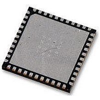
AT89LP52-20MU Atmel, AT89LP52-20MU Datasheet - Page 57

AT89LP52-20MU
Manufacturer Part Number
AT89LP52-20MU
Description
IC MCU 8051 8K FLASH SPI 44VQFN
Manufacturer
Atmel
Series
89LPr
Datasheet
1.AT89LP52-20MU.pdf
(113 pages)
Specifications of AT89LP52-20MU
Core Processor
8051
Core Size
8-Bit
Speed
20MHz
Connectivity
EBI/EMI, I²C, SPI, UART/USART
Peripherals
Brown-out Detect/Reset, POR, PWM, WDT
Number Of I /o
36
Program Memory Size
8KB (8K x 8)
Program Memory Type
FLASH
Ram Size
256 x 8
Voltage - Supply (vcc/vdd)
2.4 V ~ 5.5 V
Oscillator Type
Internal
Operating Temperature
-40°C ~ 85°C
Package / Case
44-VFQFN Exposed Pad
Processor Series
AT89x
Core
8051
Data Bus Width
8 bit
Data Ram Size
256 B
Interface Type
Serial
Maximum Clock Frequency
20 MHz
Number Of Programmable I/os
36
Number Of Timers
3
Operating Supply Voltage
2.7 V to 5.5 V
Maximum Operating Temperature
+ 85 C
Mounting Style
SMD/SMT
Lead Free Status / RoHS Status
Lead free / RoHS Compliant
Eeprom Size
-
Data Converters
-
Lead Free Status / Rohs Status
Details
Available stocks
Company
Part Number
Manufacturer
Quantity
Price
Company:
Part Number:
AT89LP52-20MU
Manufacturer:
Atmel
Quantity:
490
Table 14-1.
Notes:
3709B–MICRO–12/10
SCON Address = 98H
Bit Addressable
Bit
Symbol
FE
SM0
SM1
SM2
REN
TB8
RB8
TI
RI
(SMOD0 = 0/1)
1. SMOD0 is located at PCON.6.
2. f
SM0/FE
SYS
Function
Framing error bit. This bit is set by the receiver when an invalid stop bit is detected. The FE bit is not cleared by valid
frames and must be cleared by software. The SMOD0 bit must be set to enable access to the FE bit. FE will be set
regardless of the state of SMOD0.
Serial Port Mode Bit 0, (SMOD0 must = 0 to access bit SM0)
Serial Port Mode Bit 1
Enables the Automatic Address Recognition feature in Modes 2 or 3. If SM2 = 1 then Rl will not be set unless the received
9th data bit (RB8) is 1, indicating an address, and the received byte is a Given or Broadcast Address. In Mode 1, if SM2 =
1 then Rl will not be activated unless a valid stop bit was received, and the received byte is a Given or Broadcast Address.
In Mode 0, SM2 determines the idle state of the shift clock such that the clock is the inverse of SM2, i.e. when SM2 = 0
the clock idles high and when SM2 = 1 the clock idles low.
Enables serial reception. Set by software to enable reception. Clear by software to disable reception.
The 9th data bit that will be transmitted in Modes 2 and 3. Set or clear by software as desired. In Mode 0, setting TB8
enables Timer 1 as the shift clock generator.
In Modes 2 and 3, the 9th data bit that was received. In Mode 1, if SM2 = 0, RB8 is the stop bit that was received. In Mode
0, RB8 is not used.
Transmit interrupt flag. Set by hardware at the end of the 8th bit time in Mode 0, or at the beginning of the stop bit in the
other modes, in any serial transmission. Must be cleared by software.
Receive interrupt flag. Set by hardware at the end of the 8th bit time in Mode 0, or halfway through the stop bit time in the
other modes, in any serial reception (except see SM2). Must be cleared by software.
7
SCON – Serial Port Control Register
= system frequency. The baud rate depends on SMOD1 (PCON.7).
SM0
0
0
1
1
(1)
In all four modes, transmission is initiated by any instruction that uses SBUF as a destination
register. Reception is initiated in Mode 0 by the condition RI = 0 and REN = 1. Reception is initi-
ated in the other modes by the incoming start bit if REN = 1.
SM1
• Mode 3: 11 bits are transmitted (through TXD) or received (through RXD): a start bit (0),
6
Special Function Register SCON, while the stop bit is ignored. The baud rate is
programmable to either 1/16 or 1/32 the system frequency.
8 data bits (LSB first), a programmable 9th data bit, and a stop bit (1). In fact, Mode 3 is the
same as Mode 2 in all respects except the baud rate, which is variable based on Timer 1 or
Timer 2 in Mode 3.
SM1
0
1
0
1
SM2
5
Mode
0
1
2
3
REN
4
Description
shift register
8-bit UART
9-bit UART
9-bit UART
TB8
3
variable (Timer 1 or Timer 2)
variable (Timer 1 or Timer 2)
AT89LP51/52 - Preliminary
f
Baud Rate (Compat.)
SYS
/3 or f
f
SYS
/32 or f
SYS
RB8
2
/6 or Timer 1
SYS
/16
Reset Value = 0000 0000B
(2)
T1
1
variable (Timer 1 or Timer 2)
variable (Timer 1 or Timer 2)
f
SYS
Baud Rate (Fast)
/2 or f
f
SYS
/32 or f
SYS
RI
0
/4 or Timer 1
SYS
/16
(2)
57


