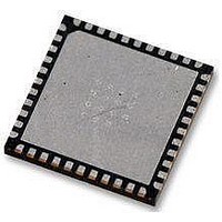
AT89LP52-20MU Atmel, AT89LP52-20MU Datasheet - Page 9

AT89LP52-20MU
Manufacturer Part Number
AT89LP52-20MU
Description
IC MCU 8051 8K FLASH SPI 44VQFN
Manufacturer
Atmel
Series
89LPr
Datasheet
1.AT89LP52-20MU.pdf
(113 pages)
Specifications of AT89LP52-20MU
Core Processor
8051
Core Size
8-Bit
Speed
20MHz
Connectivity
EBI/EMI, I²C, SPI, UART/USART
Peripherals
Brown-out Detect/Reset, POR, PWM, WDT
Number Of I /o
36
Program Memory Size
8KB (8K x 8)
Program Memory Type
FLASH
Ram Size
256 x 8
Voltage - Supply (vcc/vdd)
2.4 V ~ 5.5 V
Oscillator Type
Internal
Operating Temperature
-40°C ~ 85°C
Package / Case
44-VFQFN Exposed Pad
Processor Series
AT89x
Core
8051
Data Bus Width
8 bit
Data Ram Size
256 B
Interface Type
Serial
Maximum Clock Frequency
20 MHz
Number Of Programmable I/os
36
Number Of Timers
3
Operating Supply Voltage
2.7 V to 5.5 V
Maximum Operating Temperature
+ 85 C
Mounting Style
SMD/SMT
Lead Free Status / RoHS Status
Lead free / RoHS Compliant
Eeprom Size
-
Data Converters
-
Lead Free Status / Rohs Status
Details
Available stocks
Company
Part Number
Manufacturer
Quantity
Price
Company:
Part Number:
AT89LP52-20MU
Manufacturer:
Atmel
Quantity:
490
2.2.6
2.2.7
2.2.8
2.2.9
3709B–MICRO–12/10
Serial Port
I/O Ports
Security
Programming
The timer prescaler increases the range of achievable baud rates when using Timer 1 to gener-
ate the baud rate in UART Modes 1 or 3, including an increase in the maximum baud rate
available in Compatibility mode. Additional features include automatic address recognition and
framing error detection.
The shift register mode (Mode 0) has been enhanced with more control of the polarity, phase
and frequency of the clock and full-duplex operation. This allows emulation of master serial
pheriperal (SPI) and two-wire (TWI) interfaces.
The P0, P1, P2 and P3 I/O ports of the AT89LP51/52 may be configured in four different modes.
The default setting depends on the Tristate-Port User Fuse. When the fuse is set all the I/O ports
revert to input-only (tristated) mode at power-up or reset. When the fuse is not active, ports P1,
P2 and P3 start in quasi-bidirectional mode and P0 starts in open-drain mode. P4 always oper-
ates in quasi-bidirectional mode. P0 can be configured to have internal pull-ups by placing it in
quasi-bidirectional or output modes. This can reduce system cost by removing the need for
external pull-ups on Port 0.
The P4.4–P4.7 pins are additional I/Os that replace the normally dedicated ALE, PSEN, XTAL1
and XTAL2 pins of the AT89S51/52. These pins can be used as additional I/Os depending on
the configuration of the clock and external memory.
The AT89LP51/52 does not support the extenal access pin (EA). Therefore it is not possible to
execute from external program memory in address range 0000H–1FFFH. When the third Lockbit
is enabled (Lock Mode 4) external program execution is disabled for all addresses above
1FFFH. This differs from AT89S51/52 where Lock Mode 4 prevents EA from being sampled low,
but may still allow external execution at addresses outside the 8K internal space.
The AT89LP51/52 supports a richer command set for In-System Programming (ISP). Existing
AT89S51/52 programmers should be able to program the AT89LP51/52 in byte mode. In page
mode the AT89LP51/52 only supports programming of a half-page of 64 bytes and therefore
requires an extra address byte as compared to AT89S51/52. Furthermore the device signature
is located at addresses 0000H, 0001H and 0003H instead of 0000H, 0100H and 0200H.
Table 2-1.
Feature
Instruction Fetch in System Clocks
Instruction Execution Time in System Clocks
Default System Clock Divisor
Default Timer Prescaler Divisor
Pin Sampling Rate (INT0, INT1, T0, T1, T2, T2EX)
Minimum RST input pulse in System Clocks
WDIDLE and DISRTO bit locations
Compatibility Mode versus Fast Mode Summary
AT89LP51/52 - Preliminary
Prescaler Rate
6, 12, 18 or 24
Compatibility
AUXR
12
3
2
6
System Clock
1, 2, 3, 4 or 5
WDTCON
Fast
1
1
1
2
9


