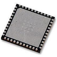
AT89LP52-20MU Atmel, AT89LP52-20MU Datasheet - Page 32

AT89LP52-20MU
Manufacturer Part Number
AT89LP52-20MU
Description
IC MCU 8051 8K FLASH SPI 44VQFN
Manufacturer
Atmel
Series
89LPr
Datasheet
1.AT89LP52-20MU.pdf
(113 pages)
Specifications of AT89LP52-20MU
Core Processor
8051
Core Size
8-Bit
Speed
20MHz
Connectivity
EBI/EMI, I²C, SPI, UART/USART
Peripherals
Brown-out Detect/Reset, POR, PWM, WDT
Number Of I /o
36
Program Memory Size
8KB (8K x 8)
Program Memory Type
FLASH
Ram Size
256 x 8
Voltage - Supply (vcc/vdd)
2.4 V ~ 5.5 V
Oscillator Type
Internal
Operating Temperature
-40°C ~ 85°C
Package / Case
44-VFQFN Exposed Pad
Processor Series
AT89x
Core
8051
Data Bus Width
8 bit
Data Ram Size
256 B
Interface Type
Serial
Maximum Clock Frequency
20 MHz
Number Of Programmable I/os
36
Number Of Timers
3
Operating Supply Voltage
2.7 V to 5.5 V
Maximum Operating Temperature
+ 85 C
Mounting Style
SMD/SMT
Lead Free Status / RoHS Status
Lead free / RoHS Compliant
Eeprom Size
-
Data Converters
-
Lead Free Status / Rohs Status
Details
Available stocks
Company
Part Number
Manufacturer
Quantity
Price
Company:
Part Number:
AT89LP52-20MU
Manufacturer:
Atmel
Quantity:
490
7.2
7.3
32
Brown-out Reset
External Reset
AT89LP51/52 - Preliminary
Table 7-1.
The AT89LP51/52 has an on-chip Brown-out Detection (BOD) circuit for monitoring the V
during operation by comparing it to a fixed trigger level. The trigger level V
nominally 2.0V. The purpose of the BOD is to ensure that if V
speed, the system will gracefully enter reset without the possibility of errors induced by incorrect
execution. A BOD sequence is shown in
trigger level V
trigger level plus about 200 mV of hysteresis, the start-up timer releases the internal reset after
the specified time-out period has expired
Figure 7-2.
The AT89LP51/52 allows for a wide V
cient to prevent incorrect execution if V
as when a 5.0V supply is coupled with high frequency operation. In such cases an external
Brown-out Reset circuit connected to the RST pin may be required.
The RST pin of the AT89LP51/52 can function as either an active-low reset input or as an active-
high reset input. The polarity of the RST pin is selectable using the POL pin (formerly EA). When
POL is high the RST pin is active high with an on-chip pull-down resistor tied to GND. When
POL is low the RST pin is active low with an on-chip pull-up resistor tied to V
structure is shown in
cycles and must be held active for at least twelve clock cycles to trigger the internal reset. In
Fast mode the reset pin is sampled every clock cycle and must be held active for at least two
clock cycles to trigger the internal reset.
SUT Fuse 1
Time-out
Internal
Reset
V
0
0
1
1
DD
BOD
Start-up Timer Settings
Brown-out Detector Reset
V POR
, the internal reset is immediately activated. When V
SUT Fuse 0
Figure
0
1
0
1
7-3. In Compatibility mode the reset pin is sampled every six clock
Clock Source
Internal RC/External Clock
Crystal Oscillator
Internal RC/External Clock
Crystal Oscillator
Internal RC/External Clock
Crystal Oscillator
Internal RC/External Clock
Crystal Oscillator
DD
BOD
Figure
(Table
operating range. The on-chip BOD may not be suffi-
is lower than the minimum required V
V BOD
t SUT
7-1).
7-2. When V
DD
DD
decreases to a value below the
fails or dips while executing at
DD
increases above the
BOD
t
SUT
DD
3709B–MICRO–12/10
for the BOD is
DD
. The RST pin
16384
(± 5%) µs
1024
2048
1024
4096
4096
512
16
range, such
DD
level


