AT89LP52-20MU Atmel, AT89LP52-20MU Datasheet - Page 36
AT89LP52-20MU
Manufacturer Part Number
AT89LP52-20MU
Description
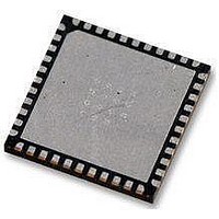
IC MCU 8051 8K FLASH SPI 44VQFN
Manufacturer
Atmel
Series
89LPr
Datasheet
1.AT89LP52-20MU.pdf
(113 pages)
Specifications of AT89LP52-20MU
Core Processor
8051
Core Size
8-Bit
Speed
20MHz
Connectivity
EBI/EMI, I²C, SPI, UART/USART
Peripherals
Brown-out Detect/Reset, POR, PWM, WDT
Number Of I /o
36
Program Memory Size
8KB (8K x 8)
Program Memory Type
FLASH
Ram Size
256 x 8
Voltage - Supply (vcc/vdd)
2.4 V ~ 5.5 V
Oscillator Type
Internal
Operating Temperature
-40°C ~ 85°C
Package / Case
44-VFQFN Exposed Pad
Processor Series
AT89x
Core
8051
Data Bus Width
8 bit
Data Ram Size
256 B
Interface Type
Serial
Maximum Clock Frequency
20 MHz
Number Of Programmable I/os
36
Number Of Timers
3
Operating Supply Voltage
2.7 V to 5.5 V
Maximum Operating Temperature
+ 85 C
Mounting Style
SMD/SMT
Lead Free Status / RoHS Status
Lead free / RoHS Compliant
Eeprom Size
-
Data Converters
-
Lead Free Status / Rohs Status
Details
Available stocks
Company
Part Number
Manufacturer
Quantity
Price
Company:

Part Number:
AT89LP52-20MU
Manufacturer:
Atmel
Quantity:
490


8.3
9. Interrupts
36
Reducing Power Consumption
AT89LP51/52 - Preliminary
Figure 8-3.
Several possibilities need consideration when trying to reduce the power consumption in an
8051-based system. Generally, Idle or Power-down mode should be used as often as possible.
All unneeded functions should be disabled. The System Clock Divider can scale down the oper-
ating frequency during periods of low demand. The ALE output can be disabled by setting
DISALE in AUXR, thereby also reducing EMI.
The AT89LP51/52 provides 6 interrupt sources: two external interrupts, three timer interrupts,
and a serial port interrupt. These interrupts and the system reset each have a separate program
vector at the start of the program memory space. Each interrupt source can be individually
enabled or disabled by setting or clearing a bit in the interrupt enable register IE. The IE register
also contains a global disable bit, EA, which disables all interrupts.
Each interrupt source can be individually programmed to one of four priority levels by setting or
clearing bits in the interrupt priority registers IP and IPH. IP holds the low order priority bits and
IPH holds the high priority bits for each interrupt. An interrupt service routine in progress can be
interrupted by a higher priority interrupt, but not by another interrupt of the same or lower priority.
The highest priority interrupt cannot be interrupted by any other interrupt source. If two requests
of different priority levels are pending at the end of an instruction, the request of higher priority
level is serviced. If requests of the same priority level are pending at the end of an instruction, an
internal polling sequence determines which request is serviced. The polling sequence is based
on the vector address; an interrupt with a lower vector address has higher priority than an inter-
rupt with a higher vector address. Note that the polling sequence is only used to resolve pending
requests of the same priority level.
The External Interrupts INT0 and INT1 can each be either level-activated or edge-activated,
depending on bits IT0 and IT1 in Register TCON. The flags that actually generate these inter-
rupts are the IE0 and IE1 bits in TCON. When the service routine is vectored to, hardware clears
the flag that generated an external interrupt only if the interrupt was edge-activated. If the inter-
rupt was level activated, then the external requesting source (rather than the on-chip hardware)
controls the request flag.
The Timer 0 and Timer 1 Interrupts are generated by TF0 and TF1, which are set by a rollover in
their respective Timer/Counter registers (except for Timer 0 in Mode 3). When a timer interrupt is
generated, the on-chip hardware clears the flag that generated it when the service routine is
Internal
Internal
XTAL1
Reset
Clock
PWD
RST
Reset Recovery from Power-down (POL = 1)
t SUT
3709B–MICRO–12/10
Related parts for AT89LP52-20MU
Image
Part Number
Description
Manufacturer
Datasheet
Request
R

Part Number:
Description:
Manufacturer:
Atmel Corporation
Datasheet:

Part Number:
Description:
IC MCU 8051 8K FLASH SPI 44TQFP
Manufacturer:
Atmel
Datasheet:

Part Number:
Description:
IC MCU 8051 8K FLASH SPI 44PLCC
Manufacturer:
Atmel
Datasheet:

Part Number:
Description:
IC MCU 8051 8K FLASH SPI 40PDIP
Manufacturer:
Atmel
Datasheet:

Part Number:
Description:
DEV KIT FOR AVR/AVR32
Manufacturer:
Atmel
Datasheet:
Part Number:
Description:
INTERVAL AND WIPE/WASH WIPER CONTROL IC WITH DELAY
Manufacturer:
ATMEL Corporation
Datasheet:
Part Number:
Description:
Low-Voltage Voice-Switched IC for Hands-Free Operation
Manufacturer:
ATMEL Corporation
Datasheet:
Part Number:
Description:
MONOLITHIC INTEGRATED FEATUREPHONE CIRCUIT
Manufacturer:
ATMEL Corporation
Datasheet:
Part Number:
Description:
AM-FM Receiver IC U4255BM-M
Manufacturer:
ATMEL Corporation
Datasheet:
Part Number:
Description:
Monolithic Integrated Feature Phone Circuit
Manufacturer:
ATMEL Corporation
Datasheet:
Part Number:
Description:
Multistandard Video-IF and Quasi Parallel Sound Processing
Manufacturer:
ATMEL Corporation
Datasheet:
Part Number:
Description:
High-performance EE PLD
Manufacturer:
ATMEL Corporation
Datasheet: