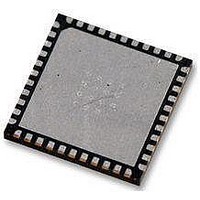
AT89LP52-20MU Atmel, AT89LP52-20MU Datasheet - Page 56

AT89LP52-20MU
Manufacturer Part Number
AT89LP52-20MU
Description
IC MCU 8051 8K FLASH SPI 44VQFN
Manufacturer
Atmel
Series
89LPr
Datasheet
1.AT89LP52-20MU.pdf
(113 pages)
Specifications of AT89LP52-20MU
Core Processor
8051
Core Size
8-Bit
Speed
20MHz
Connectivity
EBI/EMI, I²C, SPI, UART/USART
Peripherals
Brown-out Detect/Reset, POR, PWM, WDT
Number Of I /o
36
Program Memory Size
8KB (8K x 8)
Program Memory Type
FLASH
Ram Size
256 x 8
Voltage - Supply (vcc/vdd)
2.4 V ~ 5.5 V
Oscillator Type
Internal
Operating Temperature
-40°C ~ 85°C
Package / Case
44-VFQFN Exposed Pad
Processor Series
AT89x
Core
8051
Data Bus Width
8 bit
Data Ram Size
256 B
Interface Type
Serial
Maximum Clock Frequency
20 MHz
Number Of Programmable I/os
36
Number Of Timers
3
Operating Supply Voltage
2.7 V to 5.5 V
Maximum Operating Temperature
+ 85 C
Mounting Style
SMD/SMT
Lead Free Status / RoHS Status
Lead free / RoHS Compliant
Eeprom Size
-
Data Converters
-
Lead Free Status / Rohs Status
Details
Available stocks
Company
Part Number
Manufacturer
Quantity
Price
Company:
Part Number:
AT89LP52-20MU
Manufacturer:
Atmel
Quantity:
490
13. External Interrupts
14. Serial Interface (UART)
56
AT89LP51/52 - Preliminary
The INT0 (P3.2) and INT1 (P3.3) pins of the AT89LP51/52 may be used as external interrupt
sources. The external interrupts can be programmed to be level-activated or transition-activated
by setting or clearing bit IT1 or IT0 in Register TCON. If ITx = 0, external interrupt x is triggered
by a detected low at the INTx pin. If ITx = 1, external interrupt x is edge-triggered. In this mode if
successive samples of the INTx pin show a high in one cycle and a low in the next cycle, inter-
rupt request flag IEx in TCON is set. Flag bit IEx then requests the interrupt. Since the external
interrupt pins are sampled once each clock cycle, an input high or low should hold for at least 2
system periods to ensure sampling. If the external interrupt is transition-activated, the external
source has to hold the request pin high for at least two clock cycles, and then hold it low for at
least two clock cycles to ensure that the transition is seen so that interrupt request flag IEx will
be set. IEx will be automatically cleared by the CPU when the service routine is called if gener-
ated in edge-triggered mode. If the external interrupt is level-activated, the external source has
to hold the request active until the requested interrupt is actually generated. Then the external
source must deactivate the request before the interrupt service routine is completed, or else
another interrupt will be generated. Both INT0 and INT1 may wake up the device from the
Power-down state.
The serial interface on the AT89LP51/52 implements a Universal Asynchronous
Receiver/Transmitter (UART). The UART has the following features:
The serial interface is full-duplex, which means it can transmit and receive simultaneously. It is
also receive-buffered, which means it can begin receiving a second byte before a previously
received byte has been read from the receive register. (However, if the first byte still has not
been read when reception of the second byte is complete, one of the bytes will be lost.) The
serial port receive and transmit registers are both accessed at the Special Function Register
SBUF. Writing to SBUF loads the transmit register, and reading SBUF accesses a physically
separate receive register. The serial port can operate in the following four modes.
• Full-duplex Operation
• 8 or 9 Data Bits
• Framing Error Detection
• Multiprocessor Communication Mode with Automatic Address Recognition
• Baud Rate Generator Using Timer 1 or Timer 2
• Interrupt on Receive Buffer Full or Transmission Complete
• Synchronous SPI or TWI Master Emulation
• Mode 0: Serial data enters and exits through RXD. TXD outputs the shift clock. Eight data
• Mode 1: 10 bits are transmitted (through TXD) or received (through RXD): a start bit (0),
• Mode 2: 11 bits are transmitted (through TXD) or received (through RXD): a start bit (0),
bits are transmitted/received, with the LSB first. The baud rate is programmable to 1/6 or 1/3
the system frequency in Compatibility mode, 1/4 or 1/2 the system frequency in Fast mode,
or variable based on Time 1.
8 data bits (LSB first), and a stop bit (1). On receive, the stop bit goes into RB8 in the Special
Function Register SCON. The baud rate is variable based on Timer 1 or Timer 2.
8 data bits (LSB first), a programmable 9th data bit, and a stop bit (1). On transmit, the 9th
data bit (TB8 in SCON) can be assigned the value of “0” or “1”. For example, the parity bit
(P, in the PSW) can be moved into TB8. On receive, the 9th data bit goes into RB8 in the
3709B–MICRO–12/10


