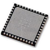
AT89LP52-20MU Atmel, AT89LP52-20MU Datasheet - Page 25

AT89LP52-20MU
Manufacturer Part Number
AT89LP52-20MU
Description
IC MCU 8051 8K FLASH SPI 44VQFN
Manufacturer
Atmel
Series
89LPr
Datasheet
1.AT89LP52-20MU.pdf
(113 pages)
Specifications of AT89LP52-20MU
Core Processor
8051
Core Size
8-Bit
Speed
20MHz
Connectivity
EBI/EMI, I²C, SPI, UART/USART
Peripherals
Brown-out Detect/Reset, POR, PWM, WDT
Number Of I /o
36
Program Memory Size
8KB (8K x 8)
Program Memory Type
FLASH
Ram Size
256 x 8
Voltage - Supply (vcc/vdd)
2.4 V ~ 5.5 V
Oscillator Type
Internal
Operating Temperature
-40°C ~ 85°C
Package / Case
44-VFQFN Exposed Pad
Processor Series
AT89x
Core
8051
Data Bus Width
8 bit
Data Ram Size
256 B
Interface Type
Serial
Maximum Clock Frequency
20 MHz
Number Of Programmable I/os
36
Number Of Timers
3
Operating Supply Voltage
2.7 V to 5.5 V
Maximum Operating Temperature
+ 85 C
Mounting Style
SMD/SMT
Lead Free Status / RoHS Status
Lead free / RoHS Compliant
Eeprom Size
-
Data Converters
-
Lead Free Status / Rohs Status
Details
Available stocks
Company
Part Number
Manufacturer
Quantity
Price
Company:
Part Number:
AT89LP52-20MU
Manufacturer:
Atmel
Quantity:
490
5.2
5.3
3709B–MICRO–12/10
Compatibility Mode
Enhanced Dual Data Pointers
Compatibility (12-Clock) mode is enabled by default from the factory or by setting the Compati-
bility User Fuse. In Compatibility mode instruction bytes are fetched every three system clock
cycles and the CPU operates with 6-state machine cycles and a divide-by-2 system clock for 12
oscillator periods per machine cycle. Standard instructions execute in1, 2 or 4 machine cycles.
Instruction timing in this mode is compatible with standard 8051s such as the AT89S51/52.
Compatibility mode can be used to preserve the execution profiles of legacy applications. For a
summary of differences between Fast and Compatibility modes see
ples of Compatibility mode instructions are shown in
Figure 5-2.
The AT89LP51/52 provides two 16-bit data pointers: DPTR0 formed by the register pair DPOL
and DPOH (82H an 83H), and DPTR1 formed by the register pair DP1L and DP1H (84H and
85H). The data pointers are used by several instructions to access the program or data memo-
ries. The Data Pointer Configuration Register (AUXR1) controls operation of the dual data
pointers
referenced by instructions including the DPTR operand. Each data pointer may be accessed at
its respective SFR addresses regardless of the DPS value. The AT89LP51/52 provides two
methods for fast context switching of the data pointers:
(A) 1-byte, 1-cycle instruction, e.g., INC A A
(B) 2-byte, 1-cycle instruction, e.g., ADD A, #data
(B) 2-byte, 1-cycle instruction, e.g., ADD A, #data
(C) 1-byte, 2-cycle instruction, e.g., INC DPTR
(C) 1-byte, 2-cycle instruction, e.g., INC DPTR
(D) MOVX (1-byte, 2-cycle)
(D) MOVX (1-byte, 2-cycle)
CLK
CLK
ALE
ALE
(Table 5-3 on page
Instruction Execution Sequences in Compatibility Mode
S1
S1
S1
S1
S1
S1
S1
S1
S1
S1
READ OPCODE
READ OPCODE
READ OPCODE
READ OPCODE
READ
READ
OPCODE
OPCODE
(MOVX)
(MOVX)
READ OPCODE
READ OPCODE
S2
S2
S2
S2
S2
S2
S2
S2
S2
S2
27). The DPS bit in AUXR1 selects which data pointer is currently
S3
S3
S3
S3
S3
S3
S3
S3
S3
S3
READ NEXT
READ NEXT
OPCODE (DISCARD)
OPCODE (DISCARD)
S4
S4
S4
S4
S4
S4
S4
S4
S4
S4
READ NEXT
READ NEXT
OPCODE
OPCODE
(DISCARD)
(DISCARD)
READ 2ND
READ 2ND
BYTE
BYTE
ACCESS EXTERNAL MEMOR
ACCESS EXTERNAL MEMORY
ADDR
ADDR
S5
S5
S5
S5
S5
S5
S5
S5
S5
S5
AT89LP51/52 - Preliminary
READ NEXT
READ NEXT
OPCODE (DISCARD)
OPCODE (DISCARD)
S6
S6
S6
S6
S6
S6
S6
S6
S6
S6
FETCH
FETCH
Figure
S1
S1
S1
S1
S1
S1
NO
NO
DA
DATA
READ NEXT OPCODE AGAIN
READ NEXT OPCODE AGAIN
READ NEXT OPCODE
READ NEXT OPCODE
S2
S2
S2
S2
S2
S2
5-2.
NO
NO
ALE
ALE
S3
S3
S3
S3
S3
S3
FETCH
FETCH
Table 2-1 on page
NO
NO
S4
S4
S4
S4
S4
S4
OPCODE AGAIN
OPCODE AGAIN
READ NEXT
READ NEXT
READ NEXT
READ NEXT
S5
S5
S5
S5
S5
S5
OPCODE
OPCODE
AGAIN
AGAIN
S6
S6
S6
S6
S6
S6
S1
S1
9. Exam-
25


