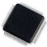
UPD78F0890GK(A)-GAJ-AX NEC, UPD78F0890GK(A)-GAJ-AX Datasheet - Page 183

UPD78F0890GK(A)-GAJ-AX
Manufacturer Part Number
UPD78F0890GK(A)-GAJ-AX
Description
8BIT MCU, 128K FLASH, 7K RAM, LQFP
Manufacturer
NEC
Datasheet
1.UPD78F0890GKA-GAJ-AX.pdf
(732 pages)
Specifications of UPD78F0890GK(A)-GAJ-AX
Controller Family/series
UPD78F
No. Of I/o's
55
Ram Memory Size
7KB
Cpu Speed
20MHz
No. Of Timers
10
No. Of Pwm
RoHS Compliant
Core Size
8bit
Program Memory Size
128KB
Oscillator Type
External, Internal
- Current page: 183 of 732
- Download datasheet (4Mb)
Address: FFA5H
Symbol
TOC02
The value of this bit is always 0 when it is read. Do not set this bit to 1 in a mode other than the one-shot
pulse output mode.
If it is set to 1, TM02 is cleared and started.
One-shot pulse output operates correctly in the free-running timer mode or clear & start mode entered by
TI002 pin valid edge input.
The one-shot pulse cannot be output in the clear & start mode entered upon a match between TM02 and
CR002.
The interrupt signal (INTTM012) is generated even when TOC024 = 0.
• LVS02 and LVR02 can be used to set the initial value of the output level of the TO02 pin. If the initial
• Be sure to set LVS02 and LVR02 when TOE02 = 1.
• LVS02 and LVR02 are trigger bits. By setting these bits to 1, the initial value of the output level of the
The interrupt signal (INTTM002) is generated even when TOC012 = 0.
• The values of LVS02 and LVR02 are always 0 when they are read.
• For how to set LVS02 and LVR02, see 7.5.2 Setting LVS0n and LVR0n.
OSPT02
OSPE02
TOC024
TOC021
TOE02
LVS02
value does not have to be set, leave LVS02 and LVR02 as 00.
LVS02, LVR02, and TOE02 being simultaneously set to 1 is prohibited.
TO02 pin can be set. Even if these bits are cleared to 0, output of the TO02 pin is not affected.
Figure 7-19. Format of 16-Bit Timer Output Control Register 02 (TOC02)
7
0
0
1
0
1
0
1
0
0
1
1
0
1
0
1
After reset: 00H
One-shot pulse output
Successive pulse output
One-shot pulse output
Disables inversion operation
Enables inversion operation
Disables inversion operation
Enables inversion operation
Disables output (TO02 pin output is fixed to low level)
Enables output
CHAPTER 7 16-BIT TIMER/EVENT COUNTERS 00 TO 03
OSPT02
LVR02
<6>
0
1
0
1
R/W
No change
Initial value of TO02 pin output is low level (TO02 pin output is cleared to 0).
Initial value of TO02 pin output is high level (TO02 pin output is set to 1).
Setting prohibited
OSPE02
TO02 pin output control on match between CR012 and TM02
TO02 pin output control on match between CR002 and TM02
<5>
User’s Manual U17554EJ4V0UD
One-shot pulse output trigger via software
One-shot pulse output operation control
TOC024
4
TO02 pin output control
Setting of TO02 pin output status
LVS02
<3>
−
LVR02
<2>
TOC021
1
TOE02
<0>
183
Related parts for UPD78F0890GK(A)-GAJ-AX
Image
Part Number
Description
Manufacturer
Datasheet
Request
R

Part Number:
Description:
16/8 bit single-chip microcomputer
Manufacturer:
NEC
Datasheet:

Part Number:
Description:
Dual audio power amp circuit
Manufacturer:
NEC
Datasheet:

Part Number:
Description:
Dual comparator
Manufacturer:
NEC
Datasheet:

Part Number:
Description:
MOS type composite field effect transistor
Manufacturer:
NEC
Datasheet:

Part Number:
Description:
50 V/100 mA FET array incorporating 2 N-ch MOSFETs
Manufacturer:
NEC
Datasheet:

Part Number:
Description:
6-pin small MM high-frequency double transistor
Manufacturer:
NEC
Datasheet:

Part Number:
Description:
6-pin small MM high-frequency double transistor
Manufacturer:
NEC
Datasheet:

Part Number:
Description:
6-pin small MM high-frequency double transistor
Manufacturer:
NEC
Datasheet:

Part Number:
Description:
6-pin small MM high-frequency double transistor
Manufacturer:
NEC
Datasheet:

Part Number:
Description:
Twin transistors equipped with different model chips(6P small MM)
Manufacturer:
NEC
Datasheet:

Part Number:
Description:
Bipolar analog integrated circuit
Manufacturer:
NEC
Datasheet:


