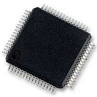
UPD78F0890GK(A)-GAJ-AX NEC, UPD78F0890GK(A)-GAJ-AX Datasheet - Page 49

UPD78F0890GK(A)-GAJ-AX
Manufacturer Part Number
UPD78F0890GK(A)-GAJ-AX
Description
8BIT MCU, 128K FLASH, 7K RAM, LQFP
Manufacturer
NEC
Datasheet
1.UPD78F0890GKA-GAJ-AX.pdf
(732 pages)
Specifications of UPD78F0890GK(A)-GAJ-AX
Controller Family/series
UPD78F
No. Of I/o's
55
Ram Memory Size
7KB
Cpu Speed
20MHz
No. Of Timers
10
No. Of Pwm
RoHS Compliant
Core Size
8bit
Program Memory Size
128KB
Oscillator Type
External, Internal
- Current page: 49 of 732
- Download datasheet (4Mb)
(2) CALLT instruction table area
(3) Option byte area
(4) CALLF instruction entry area
(5) On-chip debug security ID setting area
3.1.2 Bank area (
The
The banks are selected by a bank select register (BANK) (see 4.3 Memory Bank Select Register (BANK)).
(a)
The 64-byte area 0040H to 007FH can store the subroutine entry address of a 1-byte call instruction (CALLT).
The option byte area is assigned to the 1-byte area of 0080H. Refer to CHAPTER 23 OPTION BYTE for details.
The area 0800H to 0FFFH can perform a direct subroutine call with a 2-byte call instruction (CALLF).
A 10-byte area of 0085H to 008EH and 1085H to 108EH can be used as an on-chip debug security ID setting
area. Set the on-chip debug security ID of 10 bytes at 0085H to 008EH when the boot swap is not used and at
0085H to 008EH and 1085H to 108EH when the boot swap is used. For details, see CHAPTER 25 ON-CHIP
DEBUG FUNCTION.
Cautions 1. Instructions cannot be fetched between different memory banks.
μ
μ
PD78F0889
PD78F0889 has bank areas 0 to 3 and the
2. Branch and access cannot be directly executed between different memory banks. Execute
3. Allocate interrupt servicing in the common area.
4. An instruction that extends from 7FFFH to 8000H can only be executed in memory bank 0.
B F F F H
7 F F F H
0 0 0 0 H
8 0 0 0 H
μ
branch or access between different memory banks via the common area.
PD78F0889 and 78F0890 only)
16384
Bank area 0
Figure 3-5. Internal ROM (Flash Memory) Configuration
8 bits
CHAPTER 3 CPU ARCHITECTURE
User’s Manual U17554EJ4V0UD
16384
Bank area 1
μ
PD78F0890 has bank areas 0 to 5 as illustrated below.
8 bits
Common area
32768
8 bits
16384
Bank area 2
8 bits
16384
Bank area 3
8 bits
49
Related parts for UPD78F0890GK(A)-GAJ-AX
Image
Part Number
Description
Manufacturer
Datasheet
Request
R

Part Number:
Description:
16/8 bit single-chip microcomputer
Manufacturer:
NEC
Datasheet:

Part Number:
Description:
Dual audio power amp circuit
Manufacturer:
NEC
Datasheet:

Part Number:
Description:
Dual comparator
Manufacturer:
NEC
Datasheet:

Part Number:
Description:
MOS type composite field effect transistor
Manufacturer:
NEC
Datasheet:

Part Number:
Description:
50 V/100 mA FET array incorporating 2 N-ch MOSFETs
Manufacturer:
NEC
Datasheet:

Part Number:
Description:
6-pin small MM high-frequency double transistor
Manufacturer:
NEC
Datasheet:

Part Number:
Description:
6-pin small MM high-frequency double transistor
Manufacturer:
NEC
Datasheet:

Part Number:
Description:
6-pin small MM high-frequency double transistor
Manufacturer:
NEC
Datasheet:

Part Number:
Description:
6-pin small MM high-frequency double transistor
Manufacturer:
NEC
Datasheet:

Part Number:
Description:
Twin transistors equipped with different model chips(6P small MM)
Manufacturer:
NEC
Datasheet:

Part Number:
Description:
Bipolar analog integrated circuit
Manufacturer:
NEC
Datasheet:


