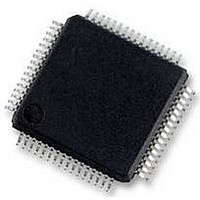
UPD78F0890GK(A)-GAJ-AX NEC, UPD78F0890GK(A)-GAJ-AX Datasheet - Page 626

UPD78F0890GK(A)-GAJ-AX
Manufacturer Part Number
UPD78F0890GK(A)-GAJ-AX
Description
8BIT MCU, 128K FLASH, 7K RAM, LQFP
Manufacturer
NEC
Datasheet
1.UPD78F0890GKA-GAJ-AX.pdf
(732 pages)
Specifications of UPD78F0890GK(A)-GAJ-AX
Controller Family/series
UPD78F
No. Of I/o's
55
Ram Memory Size
7KB
Cpu Speed
20MHz
No. Of Timers
10
No. Of Pwm
RoHS Compliant
Core Size
8bit
Program Memory Size
128KB
Oscillator Type
External, Internal
- Current page: 626 of 732
- Download datasheet (4Mb)
(2) Flash protect command register (PFCMD)
(3) Flash status register (PFS)
626
If the application system stops inadvertently due to malfunction caused by noise or program hang-up, an
operation to write the flash programming mode control register (FLPMC) may have a serious effect on the system.
PFCMD is used to protect FLPMC from being written, so that the application system does not stop inadvertently.
Writing FLPMC is enabled only when a write operation is performed in the following specific sequence.
<1> Write a specific value to PFCMD (PFCMD = A5H)
<2> Write the value to be set to FLPMC (writing in this step is invalid)
<3> Write the inverted value of the value to be set to FLPMC
<4> Write the value to be set to FLPMC (writing in this step is valid)
This rewrites the value of the register, so that the register cannot be written illegally.
Occurrence of an illegal store operation can be checked by bit 0 (FPRERR) of the flash status register (PFS).
A5H must be written to PFCMD each time the value of FLPMC is changed.
PFCMD can be set by an 8-bit memory manipulation instruction.
Reset signal generation makes this register undefined.
If data is not written to the flash programming mode control register (FLPMC), which is protected, in the correct
sequence (writing the flash protect command register (PFCMD)), FLPMC is not written and a protection error
occurs. If this happens, bit 0 of PFS (FPRERR) is set to 1.
This bit is a cumulative flag. After checking FPRERR, clear it by writing 0 to it.
PFS can be set by a 1-bit or 8-bit memory manipulation instruction.
Reset signal generation clears this register to 00H.
Address: FFC0H
Address: FFC2H
PFCMD
Symbol
Symbol
PFS
Figure 24-18. Format of Flash Protect Command Register (PFCMD)
REG7
0
Figure 24-19. Format of Flash Status Register (PFS)
After reset: Undefined
After reset: 00H
REG6
0
CHAPTER 24 FLASH MEMORY
User’s Manual U17554EJ4V0UD
REG5
0
R/W
REG4
0
W
REG3
0
REG2
0
REG1
0
FPRERR
REG0
Related parts for UPD78F0890GK(A)-GAJ-AX
Image
Part Number
Description
Manufacturer
Datasheet
Request
R

Part Number:
Description:
16/8 bit single-chip microcomputer
Manufacturer:
NEC
Datasheet:

Part Number:
Description:
Dual audio power amp circuit
Manufacturer:
NEC
Datasheet:

Part Number:
Description:
Dual comparator
Manufacturer:
NEC
Datasheet:

Part Number:
Description:
MOS type composite field effect transistor
Manufacturer:
NEC
Datasheet:

Part Number:
Description:
50 V/100 mA FET array incorporating 2 N-ch MOSFETs
Manufacturer:
NEC
Datasheet:

Part Number:
Description:
6-pin small MM high-frequency double transistor
Manufacturer:
NEC
Datasheet:

Part Number:
Description:
6-pin small MM high-frequency double transistor
Manufacturer:
NEC
Datasheet:

Part Number:
Description:
6-pin small MM high-frequency double transistor
Manufacturer:
NEC
Datasheet:

Part Number:
Description:
6-pin small MM high-frequency double transistor
Manufacturer:
NEC
Datasheet:

Part Number:
Description:
Twin transistors equipped with different model chips(6P small MM)
Manufacturer:
NEC
Datasheet:

Part Number:
Description:
Bipolar analog integrated circuit
Manufacturer:
NEC
Datasheet:


