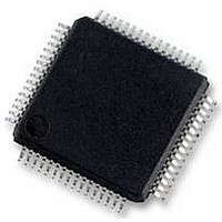
UPD78F0890GK(A)-GAJ-AX NEC, UPD78F0890GK(A)-GAJ-AX Datasheet - Page 728

UPD78F0890GK(A)-GAJ-AX
Manufacturer Part Number
UPD78F0890GK(A)-GAJ-AX
Description
8BIT MCU, 128K FLASH, 7K RAM, LQFP
Manufacturer
NEC
Datasheet
1.UPD78F0890GKA-GAJ-AX.pdf
(732 pages)
Specifications of UPD78F0890GK(A)-GAJ-AX
Controller Family/series
UPD78F
No. Of I/o's
55
Ram Memory Size
7KB
Cpu Speed
20MHz
No. Of Timers
10
No. Of Pwm
RoHS Compliant
Core Size
8bit
Program Memory Size
128KB
Oscillator Type
External, Internal
- Current page: 728 of 732
- Download datasheet (4Mb)
728
3rd
Edition
• Change of Figure and Note 2, 4
• Addition of Note 1, 3
• Change of Figure and Note 2
• Addition of Note 1 and Caution 2
• Change of Figure and Note 3
• Change of Figure 22-7 and Note 2
• Change of Figure 22-8 and Note 2
• Change of Figure 24-4
• Addition of Note
Figure 21-2. Timing of Generation of Internal Reset Signal by Power-on-Clear Circuit and Low-Voltage
Detector (1/2)
Figure 21-2. Timing of Generation of Internal Reset Signal by Power-on-Clear Circuit and Low-Voltage
Detector (2/2)
Change of Figure 21-3. Example of Software Processing After Reset Release (1/2)
Change of explanation in 22.1 Functions of Low-Voltage Detector
Change of Figure 22-1. Block Diagram of Low-Voltage Detector
Figure 22-2. Format of Low-Voltage Detection Register (LVIM)
Change of Caution 3 in Figure 22-3. Format of Low-Voltage Detection Level Selection Register (LVIS)
Change of explanation and Remark in 22.4 Operation of Low-Voltage Detector
Change of explanation in 22.4.1 (1) When detecting level of supply voltage (V
Change of explanation and Note 2 in 22.4.2 (2) When detecting level of input voltage from external input pin
(EXLVI)
Change of Figure 22-6. Timing of Low-Voltage Detector Internal Reset Signal Generation (Detects Level of
Input Voltage from External Input Pin (EXLVI))
Change of explanation in 22.4.1 (1) When detecting level of supply voltage (V
Figure 22-7. Timing of Low-Voltage Detector Interrupt Signal Generation (Detects Level of Supply Voltage
(V
Change of explanation in 22.4.2 (2) When detecting level of input voltage from external input pin (EXLVI)
Figure 22-8. Timing of Low-Voltage Detector Interrupt Signal Generation (Detects Level of Input Voltage from
External Input Pin (EXLVI))
Change of explanation in 22.5 Cautions for Low-Voltage Detector
Change of Figure 22-9. Example of Software Processing After Reset Release (1/2)
Change of CHAPTER 23 OPTION BYTE
Addition of Caution in 24.1 Internal Memory Size Switching Register
Addition of Caution in 24.2 Internal Expansion RAM Size Switching Register
Change of Note 2 in Table 24-3. Wiring Between 78K0/FE2 and Dedicated Flash Memory Programmer
Change of Figure 24-3. Example of Wiring Adapter for Flash Memory Writing in 3-Wire Serial I/O (CSI10) Mode
Figure 24-4. Example of Wiring Adapter for Flash Memory Writing in UART (UART60) Mode
Change of explanation in 24.5 (1) CSI10
Change of Figure 24-6. Communication with Dedicated Flash Memory Programmer (CSI10)
DD
))
APPENDIX D REVISION HISTORY
User’s Manual U17554EJ4V0UD
Description
DD
DD
)
)
(7/9)
Related parts for UPD78F0890GK(A)-GAJ-AX
Image
Part Number
Description
Manufacturer
Datasheet
Request
R

Part Number:
Description:
16/8 bit single-chip microcomputer
Manufacturer:
NEC
Datasheet:

Part Number:
Description:
Dual audio power amp circuit
Manufacturer:
NEC
Datasheet:

Part Number:
Description:
Dual comparator
Manufacturer:
NEC
Datasheet:

Part Number:
Description:
MOS type composite field effect transistor
Manufacturer:
NEC
Datasheet:

Part Number:
Description:
50 V/100 mA FET array incorporating 2 N-ch MOSFETs
Manufacturer:
NEC
Datasheet:

Part Number:
Description:
6-pin small MM high-frequency double transistor
Manufacturer:
NEC
Datasheet:

Part Number:
Description:
6-pin small MM high-frequency double transistor
Manufacturer:
NEC
Datasheet:

Part Number:
Description:
6-pin small MM high-frequency double transistor
Manufacturer:
NEC
Datasheet:

Part Number:
Description:
6-pin small MM high-frequency double transistor
Manufacturer:
NEC
Datasheet:

Part Number:
Description:
Twin transistors equipped with different model chips(6P small MM)
Manufacturer:
NEC
Datasheet:

Part Number:
Description:
Bipolar analog integrated circuit
Manufacturer:
NEC
Datasheet:


