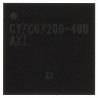
CY7C67200-48BAXI Cypress Semiconductor Corp, CY7C67200-48BAXI Datasheet - Page 42

CY7C67200-48BAXI
Manufacturer Part Number
CY7C67200-48BAXI
Description
USB HOST/PERIPH CNTRLR 48LFBGA
Manufacturer
Cypress Semiconductor Corp
Series
EZ-OTG™r
Type
OTG Programmable USB On The Gor
Datasheet
1.CY7C67200-48BAXI.pdf
(78 pages)
Specifications of CY7C67200-48BAXI
Package / Case
48-LFBGA
Controller Type
USB Peripheral Controller
Interface
Serial
Voltage - Supply
2.7 V ~ 3.6 V, 3 V ~ 3.6 V
Current - Supply
80mA, 135mA
Operating Temperature
-40°C ~ 85°C
Mounting Type
Surface Mount
Data Rate
2 Mbps
Maximum Operating Temperature
+ 85 C
Minimum Operating Temperature
- 40 C
Mounting Style
SMD/SMT
Operating Temperature Range
- 40 C to + 85 C
Supply Current
80 mA
Supply Voltage (max)
3.6 V
Supply Voltage (min)
2.7 V
Operating Supply Voltage
2.7 V to 3.6 V
Controller Family/series
PSoC 1
Core Size
16 Bit
No. Of I/o's
25
Program Memory Size
16KB
Ram Memory Size
8KB
Cpu Speed
48MHz
No. Of Timers
2
Rohs Compliant
Yes
Lead Free Status / RoHS Status
Lead free / RoHS Compliant
For Use With
CY3663 - KIT DEV EZ-OTG/EZ-HOST
Lead Free Status / Rohs Status
Lead free / RoHS Compliant
Other names
428-2262
CY7C67200-48BAXI
CY7C67200-48BAXI
Available stocks
Company
Part Number
Manufacturer
Quantity
Price
Company:
Part Number:
CY7C67200-48BAXI
Manufacturer:
CYPRESS
Quantity:
1 500
Company:
Part Number:
CY7C67200-48BAXI
Manufacturer:
CY
Quantity:
6
Company:
Part Number:
CY7C67200-48BAXI
Manufacturer:
Cypress Semiconductor Corp
Quantity:
10 000
Part Number:
CY7C67200-48BAXI
Manufacturer:
CYPRESS/赛普拉斯
Quantity:
20 000
Company:
Part Number:
CY7C67200-48BAXIT
Manufacturer:
XAC
Quantity:
105
Company:
Part Number:
CY7C67200-48BAXIT
Manufacturer:
Cypress Semiconductor Corp
Quantity:
10 000
Part Number:
CY7C67200-48BAXIT
Manufacturer:
CYPRESS/赛普拉斯
Quantity:
20 000
Document #: 38-08014 Rev. *G
Writing a 1 to any bit will output a high voltage on the corresponding GPIO pin.
Reserved
All reserved bits must be written as ‘0’.
GPIO 0 Input Data Register [0xC020] [R]
Register Description
The GPIO 0 Input Data register reads the input data of the GPIO pins. The GPIO 0 Input Data register reads from GPIO15 to
GPIO0 while the GPIO 1 Input Data register reads from GPIO31 to GPIO19.
Every bit represents the voltage of that GPIO pin.
GPIO 1 Input Data Register [0xC026] [R]
Register Description
The GPIO 1 Input Data register reads the input data of the GPIO pins. The GPIO 0 Input Data register reads from GPIO15 to
GPIO0 while the GPIO 1 Input Data register reads from GPIO31 to GPIO19.
Every bit represents the voltage of that GPIO pin.
GPIO 0 Direction Register [0xC022] [R/W]
Bit #
Field
Read/Write
Default
Bit #
Field
Read/Write
Default
Bit #
Field
Read/Write
Default
Bit #
Field
Read/Write
Default
Bit #
Field
Read/Write
Default
Bit #
Field
Read/Write
Default
GPIO15
GPIO31
GPIO23
GPIO15
GPIO7
GPIO7
R/W
R/W
15
15
15
R
R
R
R
0
7
0
0
7
0
0
7
0
GPIO14
GPIO30
GPIO22
GPIO14
GPIO6
GPIO6
R/W
R/W
14
14
14
R
R
6
0
R
R
0
0
6
0
0
6
0
Figure 44. GPIO 0 Input Data Register
Figure 45. GPIO 1 Input Data Register
Figure 46. GPIO 0 Direction Register
GPIO13
GPIO29
GPIO21
GPIO13
GPIO5
GPIO5
R/W
R/W
13
13
13
R
R
5
0
R
R
0
0
5
0
0
5
0
GPIO12
GPIO12
GPIO20
GPIO4
GPIO4
R/W
R/W
12
12
12
R
R
4
0
R
0
0
0
4
0
4
0
-
GPIO11
GPIO19
GPIO11
GPIO3
GPIO3
R/W
R/W
11
11
11
R
R
3
0
R
0
0
0
3
0
3
0
-
Reserved
GPIO10
GPIO10
GPIO2
GPIO2
R/W
R/W
10
10
10
R
R
2
0
0
0
0
2
0
2
0
-
-
Reserved
GPIO1
GPIO9
GPIO9
GPIO1
R/W
R/W
R
1
0
R
9
0
9
0
9
0
1
0
1
0
-
-
CY7C67200
Page 42 of 78
GPIO24
GPIO0
GPIO8
GPIO8
GPIO0
R/W
R/W
R
0
0
R
R
8
0
8
0
8
0
0
0
-
0
0
[+] Feedback


