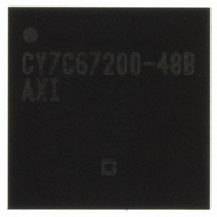
CY7C67200-48BAXI Cypress Semiconductor Corp, CY7C67200-48BAXI Datasheet - Page 43

CY7C67200-48BAXI
Manufacturer Part Number
CY7C67200-48BAXI
Description
USB HOST/PERIPH CNTRLR 48LFBGA
Manufacturer
Cypress Semiconductor Corp
Series
EZ-OTG™r
Type
OTG Programmable USB On The Gor
Datasheet
1.CY7C67200-48BAXI.pdf
(78 pages)
Specifications of CY7C67200-48BAXI
Package / Case
48-LFBGA
Controller Type
USB Peripheral Controller
Interface
Serial
Voltage - Supply
2.7 V ~ 3.6 V, 3 V ~ 3.6 V
Current - Supply
80mA, 135mA
Operating Temperature
-40°C ~ 85°C
Mounting Type
Surface Mount
Data Rate
2 Mbps
Maximum Operating Temperature
+ 85 C
Minimum Operating Temperature
- 40 C
Mounting Style
SMD/SMT
Operating Temperature Range
- 40 C to + 85 C
Supply Current
80 mA
Supply Voltage (max)
3.6 V
Supply Voltage (min)
2.7 V
Operating Supply Voltage
2.7 V to 3.6 V
Controller Family/series
PSoC 1
Core Size
16 Bit
No. Of I/o's
25
Program Memory Size
16KB
Ram Memory Size
8KB
Cpu Speed
48MHz
No. Of Timers
2
Rohs Compliant
Yes
Lead Free Status / RoHS Status
Lead free / RoHS Compliant
For Use With
CY3663 - KIT DEV EZ-OTG/EZ-HOST
Lead Free Status / Rohs Status
Lead free / RoHS Compliant
Other names
428-2262
CY7C67200-48BAXI
CY7C67200-48BAXI
Available stocks
Company
Part Number
Manufacturer
Quantity
Price
Company:
Part Number:
CY7C67200-48BAXI
Manufacturer:
CYPRESS
Quantity:
1 500
Company:
Part Number:
CY7C67200-48BAXI
Manufacturer:
CY
Quantity:
6
Company:
Part Number:
CY7C67200-48BAXI
Manufacturer:
Cypress Semiconductor Corp
Quantity:
10 000
Part Number:
CY7C67200-48BAXI
Manufacturer:
CYPRESS/赛普拉斯
Quantity:
20 000
Company:
Part Number:
CY7C67200-48BAXIT
Manufacturer:
XAC
Quantity:
105
Company:
Part Number:
CY7C67200-48BAXIT
Manufacturer:
Cypress Semiconductor Corp
Quantity:
10 000
Part Number:
CY7C67200-48BAXIT
Manufacturer:
CYPRESS/赛普拉斯
Quantity:
20 000
Document #: 38-08014 Rev. *G
Register Description
The GPIO 0 Direction register controls the direction of the GPIO data pins (input/output). The GPIO 0 Direction register controls
GPIO15 to GPIO0 while the GPIO 1 Direction register controls GPIO31 to GPIO19.
When any bit of this register is set to ‘1’, the corresponding GPIO data pin becomes an output. When any bit of this register is
set to ‘0’, the corresponding GPIO data pin becomes an input.
Reserved
All reserved bits must be written as ‘0’.
GPIO 1 Direction Register [0xC028] [R/W]
Register Description
The GPIO 1 Direction register controls the direction of the GPIO data pins (input/output). The GPIO 0 Direction register controls
GPIO15 to GPIO0 while the GPIO 1 Direction register controls GPIO31 to GPIO19.
When any bit of this register is set to ‘1’, the corresponding GPIO data pin becomes an output. When any bit of this register is
set to ‘0’, the corresponding GPIO data pin becomes an input.
Reserved
All reserved bits must be written as ‘0’.
HSS Registers
There are eight registers dedicated to HSS operation. Each of these registers are covered in this section and summarized in
Table
Table 31.HSS Registers
Bit #
Field
Read/Write
Default
Bit #
Field
Read/Write
Default
HSS Control Register
HSS Baud Rate Register
HSS Transmit Gap Register
HSS Data Register
HSS Receive Address Register
HSS Receive Length Register
HSS Transmit Address Register
HSS Transmit Length Register
31.
GPIO31
GPIO23
R/W
R/W
15
0
7
0
Register Name
GPIO30
GPIO22
R/W
R/W
14
0
6
0
Figure 47. GPIO 1 Direction Register
GPIO29
GPIO21
R/W
R/W
13
0
5
0
GPIO20
R/W
R/W
12
0
4
0
GPIO19
R/W
R/W
11
0
3
0
Reserved
Address
0xC07A
0xC07C
0xC07E
0xC070
0xC072
0xC074
0xC076
0xC078
R/W
R/W
10
0
2
0
Reserved
R/W
R/W
9
0
1
0
CY7C67200
Page 43 of 78
R/W
R/W
R/W
R/W
R/W
R/W
R/W
R/W
R/W
GPIO24
R/W
R/W
8
0
0
0
[+] Feedback


