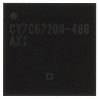
CY7C67200-48BAXI Cypress Semiconductor Corp, CY7C67200-48BAXI Datasheet - Page 50

CY7C67200-48BAXI
Manufacturer Part Number
CY7C67200-48BAXI
Description
USB HOST/PERIPH CNTRLR 48LFBGA
Manufacturer
Cypress Semiconductor Corp
Series
EZ-OTG™r
Type
OTG Programmable USB On The Gor
Datasheet
1.CY7C67200-48BAXI.pdf
(78 pages)
Specifications of CY7C67200-48BAXI
Package / Case
48-LFBGA
Controller Type
USB Peripheral Controller
Interface
Serial
Voltage - Supply
2.7 V ~ 3.6 V, 3 V ~ 3.6 V
Current - Supply
80mA, 135mA
Operating Temperature
-40°C ~ 85°C
Mounting Type
Surface Mount
Data Rate
2 Mbps
Maximum Operating Temperature
+ 85 C
Minimum Operating Temperature
- 40 C
Mounting Style
SMD/SMT
Operating Temperature Range
- 40 C to + 85 C
Supply Current
80 mA
Supply Voltage (max)
3.6 V
Supply Voltage (min)
2.7 V
Operating Supply Voltage
2.7 V to 3.6 V
Controller Family/series
PSoC 1
Core Size
16 Bit
No. Of I/o's
25
Program Memory Size
16KB
Ram Memory Size
8KB
Cpu Speed
48MHz
No. Of Timers
2
Rohs Compliant
Yes
Lead Free Status / RoHS Status
Lead free / RoHS Compliant
For Use With
CY3663 - KIT DEV EZ-OTG/EZ-HOST
Lead Free Status / Rohs Status
Lead free / RoHS Compliant
Other names
428-2262
CY7C67200-48BAXI
CY7C67200-48BAXI
Available stocks
Company
Part Number
Manufacturer
Quantity
Price
Company:
Part Number:
CY7C67200-48BAXI
Manufacturer:
CYPRESS
Quantity:
1 500
Company:
Part Number:
CY7C67200-48BAXI
Manufacturer:
CY
Quantity:
6
Company:
Part Number:
CY7C67200-48BAXI
Manufacturer:
Cypress Semiconductor Corp
Quantity:
10 000
Part Number:
CY7C67200-48BAXI
Manufacturer:
CYPRESS/赛普拉斯
Quantity:
20 000
Company:
Part Number:
CY7C67200-48BAXIT
Manufacturer:
XAC
Quantity:
105
Company:
Part Number:
CY7C67200-48BAXIT
Manufacturer:
Cypress Semiconductor Corp
Quantity:
10 000
Part Number:
CY7C67200-48BAXIT
Manufacturer:
CYPRESS/赛普拉斯
Quantity:
20 000
Document #: 38-08014 Rev. *G
SOF/EOP2 to CPU Enable (Bit 12)
The SOF/EOP2 to CPU Enable bit routes the SOF/EOP2
interrupt to the on-chip CPU. Since the SOF/EOP2 interrupt
can be routed to both the on-chip CPU and the HPI port the
firmware must ensure only one of the two (CPU, HPI) resets
the interrupt.
1: Route signal to CPU
0: Do not route signal to CPU
SOF/EOP1 to HPI Enable (Bit 11)
The SOF/EOP1 to HPI Enable bit routes the SOF/EOP1
interrupt to the HPI port.
1: Route signal to HPI port
0: Do not route signal to HPI port
SOF/EOP1 to CPU Enable (Bit 10)
The SOF/EOP1 to CPU Enable bit routes the SOF/EOP1
interrupt to the on-chip CPU. Since the SOF/EOP1 interrupt
can be routed to both the on-chip CPU and the HPI port the
firmware must ensure only one of the two (CPU, HPI) resets
the interrupt.
1: Route signal to CPU
0: Do not route signal to CPU
Reset2 to HPI Enable (Bit 9)
The Reset2 to HPI Enable bit routes the USB Reset interrupt
that occurs on Device 2 to the HPI port instead of the on-chip
CPU.
1: Route signal to HPI port
0: Do not route signal to HPI port
HPI Swap 1 Enable (Bit 8)
Both HPI Swap bits (bits 8 and 0) must be set to identical
values. When set to ‘00’, the most significant data byte goes
to HPI_D[15:8] and the least significant byte goes to
HPI_D[7:0]. This is the default setting. By setting to ‘11’, the
most significant data byte goes to HPI_D[7:0] and the least
significant byte goes to HPI_D[15:8].
Resume2 to HPI Enable (Bit 7)
The Resume2 to HPI Enable bit routes the USB Resume
interrupt that occurs on Host 2 to the HPI port instead of the
on-chip CPU.
1: Route signal to HPI port
0: Do not route signal to HPI port
Resume1 to HPI Enable (Bit 6)
The Resume1 to HPI Enable bit routes the USB Resume
interrupt that occurs on Host 1 to the HPI port instead of the
on-chip CPU.
1: Route signal to HPI port
0: Do not route signal to HPI port
Done2 to HPI Enable (Bit 3)
The Done2 to HPI Enable bit routes the Done interrupt for
Host/Device 2 to the HPI port instead of the on-chip CPU.
1: Route signal to HPI port
0: Do not route signal to HPI port
Done1 to HPI Enable (Bit 2)
The Done1 to HPI Enable bit routes the Done interrupt for
Host/Device 1 to the HPI port instead of the on-chip CPU.
1: Route signal to HPI port
0: Do not route signal to HPI port
Reset1 to HPI Enable (Bit 1)
The Reset1 to HPI Enable bit routes the USB Reset interrupt
that occurs on Device 1 to the HPI port instead of the on-chip
CPU.
1: Route signal to HPI port
0: Do not route signal to HPI port
HPI Swap 0 Enable (Bit 0)
Both HPI Swap bits (bits 8 and 0) must be set to identical
values. When set to ‘00’, the most significant data byte goes
to HPI_D[15:8] and the least significant byte goes to
HPI_D[7:0]. This is the default setting. By setting to ‘11’, the
most significant data byte goes to HPI_D[7:0] and the least
significant byte goes to HPI_D[15:8].
CY7C67200
Page 50 of 78
[+] Feedback


