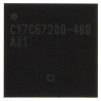
CY7C67200-48BAXI Cypress Semiconductor Corp, CY7C67200-48BAXI Datasheet - Page 55

CY7C67200-48BAXI
Manufacturer Part Number
CY7C67200-48BAXI
Description
USB HOST/PERIPH CNTRLR 48LFBGA
Manufacturer
Cypress Semiconductor Corp
Series
EZ-OTG™r
Type
OTG Programmable USB On The Gor
Datasheet
1.CY7C67200-48BAXI.pdf
(78 pages)
Specifications of CY7C67200-48BAXI
Package / Case
48-LFBGA
Controller Type
USB Peripheral Controller
Interface
Serial
Voltage - Supply
2.7 V ~ 3.6 V, 3 V ~ 3.6 V
Current - Supply
80mA, 135mA
Operating Temperature
-40°C ~ 85°C
Mounting Type
Surface Mount
Data Rate
2 Mbps
Maximum Operating Temperature
+ 85 C
Minimum Operating Temperature
- 40 C
Mounting Style
SMD/SMT
Operating Temperature Range
- 40 C to + 85 C
Supply Current
80 mA
Supply Voltage (max)
3.6 V
Supply Voltage (min)
2.7 V
Operating Supply Voltage
2.7 V to 3.6 V
Controller Family/series
PSoC 1
Core Size
16 Bit
No. Of I/o's
25
Program Memory Size
16KB
Ram Memory Size
8KB
Cpu Speed
48MHz
No. Of Timers
2
Rohs Compliant
Yes
Lead Free Status / RoHS Status
Lead free / RoHS Compliant
For Use With
CY3663 - KIT DEV EZ-OTG/EZ-HOST
Lead Free Status / Rohs Status
Lead free / RoHS Compliant
Other names
428-2262
CY7C67200-48BAXI
CY7C67200-48BAXI
Available stocks
Company
Part Number
Manufacturer
Quantity
Price
Company:
Part Number:
CY7C67200-48BAXI
Manufacturer:
CYPRESS
Quantity:
1 500
Company:
Part Number:
CY7C67200-48BAXI
Manufacturer:
CY
Quantity:
6
Company:
Part Number:
CY7C67200-48BAXI
Manufacturer:
Cypress Semiconductor Corp
Quantity:
10 000
Part Number:
CY7C67200-48BAXI
Manufacturer:
CYPRESS/赛普拉斯
Quantity:
20 000
Company:
Part Number:
CY7C67200-48BAXIT
Manufacturer:
XAC
Quantity:
105
Company:
Part Number:
CY7C67200-48BAXIT
Manufacturer:
Cypress Semiconductor Corp
Quantity:
10 000
Part Number:
CY7C67200-48BAXIT
Manufacturer:
CYPRESS/赛普拉斯
Quantity:
20 000
Document #: 38-08014 Rev. *G
SPI Control Register [0xC0CA] [R/W]
Register Description
The SPI Control register controls the SPI port. Fields apply to
both master and slave mode unless otherwise noted.
SCK Strobe (Bit 15)
The SCK Strobe bit starts the SCK strobe at the selected
frequency and polarity (set in the SPI Configuration register),
but not phase. This bit feature can only be enabled when in
master mode and must be during a period of inactivity. This bit
is self-clearing.
1: SCK Strobe Enable
0: No Function
FIFO Init (Bit 14)
The FIFO Init bit initializes the FIFO and clear the FIFO Error
Status bit. This bit is self-clearing.
1: FIFO Init Enable
0: No Function
Byte Mode (Bit 13)
The Byte Mode bit selects between PIO (byte mode) and DMA
(block mode) operation.
1: Set PIO (byte mode) operation
0: Set DMA (block mode) operation
Full Duplex (Bit 12)
The Full Duplex bit selects between full-duplex and half-duplex
operation.
1: Enable full duplex. Full duplex is not allowed and will not set
if the 3Wire Enable bit of the SPI Configuration register is set
to ‘1’
0: Enable half-duplex operation
SS Manual (Bit 11)
The SS Manual bit activates or deactivates SS if the SS Delay
Select field of the SPI Control register is all zeros and is
configured as master interface. This field only applies to
master mode.
1: Activate SS, master drives SS line asserted LOW
0: Deactivate SS, master drives SS line deasserted HIGH
Bit #
Field
Read/Write
Default
Bit #
Field
Read/Write
Default
Transmit
Strobe
Empty
SCK
15
W
R
0
7
1
Receive
FIFO
Full
Init
14
W
R
0
6
0
Figure 62. SPI Control Register
Mode
Byte
R/W
R/W
13
0
5
0
Transmit Bit Length
Full Duplex
R/W
R/W
12
0
4
0
Read Enable (Bit 10)
The Read Enable bit initiates a read phase for a master mode
transfer or set the slave to receive (in slave mode).
1: Initiates a read phase for a master transfer or sets a slave
to receive. In master mode this bit is sticky and remains set
until the read transfer begins.
0: Initiates the write phase for slave operation
Transmit Ready (Bit 9)
The Transmit Ready bit is a read-only bit that indicates if the
transmit port is ready to empty and ready to be written.
1: Ready for data to be written to the port. The transmit FIFO
is not full.
0: Not ready for data to be written to the port
Receive Data Ready (Bit 8)
The Receive Data Ready bit is a read-only bit that indicates if
the receive port has data ready.
1: Receive port has data ready to read
0: Receive port does not have data ready
Transmit Empty (Bit 7)
The Transmit Empty bit is a read-only bit that indicates if the
transmit FIFO is empty.
1: Transmit FIFO is empty
0: Transmit FIFO is not empty
Receive Full (Bit 6)
The Receive Full bit is a read-only bit that indicates if the
receive FIFO is full.
1: Receive FIFO is full
0: Receive FIFO is not full
Transmit Bit Length (Bits [5:3])
The Transmit Bit Length field controls whether a full byte or
partial byte is to be transmitted. If Transmit Bit Length is ‘000’,
a full byte is transmitted. If Transmit Bit Length is ‘001’ to ‘111’,
the value indicates the number of bits that will be transmitted.
Manual
R/W
R/w
SS
11
0
3
0
Enable
Read
R/W
R/W
10
0
2
0
Receive Bit Length
Transmit
Ready
R/w
R
9
0
1
0
CY7C67200
Page 55 of 78
Data Ready
Receive
R/W
R
8
1
0
0
[+] Feedback


