DSP56309EVM Freescale Semiconductor, DSP56309EVM Datasheet - Page 136
DSP56309EVM
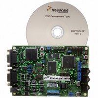
Manufacturer Part Number
DSP56309EVM
Description
KIT EVALUATION FOR XC56309
Manufacturer
Freescale Semiconductor
Type
DSPr
Specifications of DSP56309EVM
Contents
Module Board, Installation Guide, Power Supply, Cable, Software and more
Description/function
Audio DSPs
Product
Audio Modules
For Use With/related Products
DSP56309
Lead Free Status / RoHS Status
Contains lead / RoHS non-compliant


Enhanced Synchronous Serial Interface (ESSI)
output. If
Output Flag 0 (OF0) bit in the CRB. If
a receive shift register clock input. As serial Input Flag 0,
Flag 0 (IF0) bit in the ESSI Status Register (SSISR).
When
SCD0 bit value.
can be programmed as a GPIO signal (
Note:
7.2.5 Serial Control Signal (SC1)
ESSI0:SC01; ESSI1: SCI11
To determine the function of
Table 7-2. In Asynchronous mode (as for a single codec with asynchronous transmit and
receive),
signal of transmit shift register TX2, for the transmitter 0 drive-enabled signal, or for serial flag
I/O. As serial flag I/O,
together for multiple serial device selection; they can be unencoded to select up to two CODECs
or decoded externally to select up to four CODECs. If
frame sync signal, the Serial Control Direction 1 CRB[SCD1] bit determines its direction.
7-4
SYN
0
0
0
0
1
1
1
1
1
1
1
1
1
SC0
SC1
SC0
The ESSI can operate with more than one active transmitter only in Synchronous
mode.
TE0
is configured as a transmit data signal, it is always an output signal, regardless of the
0
0
1
1
0
0
0
0
0
0
0
0
1
is the receiver frame sync I/O. In Synchronous mode,
is used as the serial Output Flag 0, its value is determined by the value of the serial
Control Bits
SC0
TE1
X
X
X
X
0
0
0
0
1
1
1
1
0
is fully synchronized with the other transmit data signals (
SC1
TE2
X
X
X
X
0
0
1
1
0
0
1
1
0
operates like
Table 7-2. Mode and Signal Definitions
SC1
, select either Synchronous or Asynchronous mode, according to
RE
0
1
0
1
0
1
0
1
0
1
0
1
0
DSP56309 User’s Manual, Rev. 1
P0
SC0
SC0
) when the ESSI
RXC
RXC
F0/U
F0/U
F0/U
F0/U
SC0
TD1
TD1
TD1
TD1
U
U
U
is an input, it functions as either serial Input Flag 0 or
.
SC0
and SC1are independent flags but can be used
F1/T0D/U
F1/T0D/U
F1/T0D/U
F1/T0D/U
SC1
FSR
FSR
TD2
TD2
TD2
TD2
SC1
U
U
U
SC0
SC0
is configured as a serial flag or receive
controls the state of the serial Input
function is not in use.
ESSI Signals
SC2
FST
FST
FS
FS
FS
FS
FS
FS
FS
FS
U
U
U
SC1
is the transmitter data out
SCK
TXC
TXC
XC
XC
XC
XC
XC
XC
XC
XC
U
U
U
Freescale Semiconductor
STD
STD
TD0
TD0
TD0
and
U
U
U
U
U
U
U
U
U
U
SC1
).
SRD
RD
RD
RD
RD
RD
RD
U
U
U
U
U
U
U
SC0
Related parts for DSP56309EVM
Image
Part Number
Description
Manufacturer
Datasheet
Request
R

Part Number:
Description:
Manufacturer:
Freescale Semiconductor, Inc
Datasheet:
Part Number:
Description:
Manufacturer:
Freescale Semiconductor, Inc
Datasheet:
Part Number:
Description:
Manufacturer:
Freescale Semiconductor, Inc
Datasheet:
Part Number:
Description:
Manufacturer:
Freescale Semiconductor, Inc
Datasheet:
Part Number:
Description:
Manufacturer:
Freescale Semiconductor, Inc
Datasheet:
Part Number:
Description:
Manufacturer:
Freescale Semiconductor, Inc
Datasheet:
Part Number:
Description:
Manufacturer:
Freescale Semiconductor, Inc
Datasheet:
Part Number:
Description:
Manufacturer:
Freescale Semiconductor, Inc
Datasheet:
Part Number:
Description:
Manufacturer:
Freescale Semiconductor, Inc
Datasheet:
Part Number:
Description:
Manufacturer:
Freescale Semiconductor, Inc
Datasheet:
Part Number:
Description:
Manufacturer:
Freescale Semiconductor, Inc
Datasheet:
Part Number:
Description:
Manufacturer:
Freescale Semiconductor, Inc
Datasheet:
Part Number:
Description:
Manufacturer:
Freescale Semiconductor, Inc
Datasheet:
Part Number:
Description:
Manufacturer:
Freescale Semiconductor, Inc
Datasheet:
Part Number:
Description:
Manufacturer:
Freescale Semiconductor, Inc
Datasheet: