DSP56309EVM Freescale Semiconductor, DSP56309EVM Datasheet - Page 81
DSP56309EVM
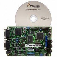
Manufacturer Part Number
DSP56309EVM
Description
KIT EVALUATION FOR XC56309
Manufacturer
Freescale Semiconductor
Type
DSPr
Specifications of DSP56309EVM
Contents
Module Board, Installation Guide, Power Supply, Cable, Software and more
Description/function
Audio DSPs
Product
Audio Modules
For Use With/related Products
DSP56309
Lead Free Status / RoHS Status
Contains lead / RoHS non-compliant


4.6.2 DRAM Control Register (DCR)
The DRAM controller is an efficient interface to dynamic RAM devices in both random
read/write cycles and Fast Access mode (Page mode). An internal DRAM controller controls the
page hit circuit, the address multiplexing (row address and column address), the control signal
generation (
DRAM module sizes and access times. The internal DRAM controller configuration is
determined by the DRAM Control Register (DCR). The DRAM Control Register (DCR) is a
24-bit read/write register that controls and configures the external DRAM accesses. The DCR
bits are shown in Figure 4-7.
Note:
Freescale Semiconductor
Number
9–5
4–0
Bit
BA1W[4–0]
Bit Name
To prevent improper device operation, you must guarantee that all the DCR bits except
BSTR are not changed during a DRAM access.
BA0W
CAS
Table 4-8. Bus Control Register (BCR) Bit Definitions (Continued)
and
Reset Value
RAS
(31 wait
(31 wait
states)
states)
11111
11111
) and the refresh access generation (
Bus Area 1 Wait State Control
Defines the number of wait states (one through 31) inserted into each external
SRAM access to Area 1 (DRAM accesses are not affected by these bits). Area 1 is
the area defined by AAR1.
Note:
When four through seven wait states are selected, one additional wait state is
inserted at the end of the access. When selecting eight or more wait states, two
additional wait states are inserted at the end of the access. These trailing wait
states increase the data hold time and the memory release time and do not
increase the memory access time.
Bus Area 0 Wait State Control
Defines the number of wait states (one through 31) inserted in each external SRAM
access to Area 0 (DRAM accesses are not affected by these bits). Area 0 is the
area defined by AAR0.
Note:
When selecting four through seven wait states, one additional wait state is inserted
at the end of the access. When selecting eight or more wait states, two additional
wait states are inserted at the end of the access. These trailing wait states increase
the data hold time and the memory release time and do not increase the memory
access time.
DSP56309 User’s Manual, Rev. 1
Do not program the value of these bits as zero, since SRAM memory
access requires at least one wait state.
Do not program the value of these bits as zero, since SRAM memory
access requires at least one wait state.
Description
CAS
before
Bus Interface Unit (BIU) Registers
RAS
) for a variety of
4-23
Related parts for DSP56309EVM
Image
Part Number
Description
Manufacturer
Datasheet
Request
R

Part Number:
Description:
Manufacturer:
Freescale Semiconductor, Inc
Datasheet:
Part Number:
Description:
Manufacturer:
Freescale Semiconductor, Inc
Datasheet:
Part Number:
Description:
Manufacturer:
Freescale Semiconductor, Inc
Datasheet:
Part Number:
Description:
Manufacturer:
Freescale Semiconductor, Inc
Datasheet:
Part Number:
Description:
Manufacturer:
Freescale Semiconductor, Inc
Datasheet:
Part Number:
Description:
Manufacturer:
Freescale Semiconductor, Inc
Datasheet:
Part Number:
Description:
Manufacturer:
Freescale Semiconductor, Inc
Datasheet:
Part Number:
Description:
Manufacturer:
Freescale Semiconductor, Inc
Datasheet:
Part Number:
Description:
Manufacturer:
Freescale Semiconductor, Inc
Datasheet:
Part Number:
Description:
Manufacturer:
Freescale Semiconductor, Inc
Datasheet:
Part Number:
Description:
Manufacturer:
Freescale Semiconductor, Inc
Datasheet:
Part Number:
Description:
Manufacturer:
Freescale Semiconductor, Inc
Datasheet:
Part Number:
Description:
Manufacturer:
Freescale Semiconductor, Inc
Datasheet:
Part Number:
Description:
Manufacturer:
Freescale Semiconductor, Inc
Datasheet:
Part Number:
Description:
Manufacturer:
Freescale Semiconductor, Inc
Datasheet: