DSP56309EVM Freescale Semiconductor, DSP56309EVM Datasheet - Page 50
DSP56309EVM
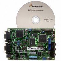
Manufacturer Part Number
DSP56309EVM
Description
KIT EVALUATION FOR XC56309
Manufacturer
Freescale Semiconductor
Type
DSPr
Specifications of DSP56309EVM
Contents
Module Board, Installation Guide, Power Supply, Cable, Software and more
Description/function
Audio DSPs
Product
Audio Modules
For Use With/related Products
DSP56309
Lead Free Status / RoHS Status
Contains lead / RoHS non-compliant


Memory Configuration
3.6 RAM Configuration Summary
The RAM configurations for the DSP56309 are listed in Table 3-1.
The actual memory locations for Program RAM and the Instruction Cache in the Program
memory space are determined by the MS and CE bits, and their addresses are given in Table 3-2.
3.7 Memory Maps
The following figures describe each of the memory space and RAM configurations defined by
the settings of the SC, MS, and CE bits. The figures show the configuration and the table
describes the bit settings, memory sizes, and memory locations.
3-6
MS
0
0
1
1
MS
0
0
1
1
Bit Settings
Table 3-2. DSP56309 RAM Address Ranges by Configuration
CE
0
1
0
1
CE
0
1
0
1
Program RAM Location
Table 3-1. DSP56309 RAM Configurations
$0000–$4FFF
$0000–$4BFF
$0000–$5FFF
$0000–$5BFF
Program RAM
DSP56309 User’s Manual, Rev. 1
20
19
24
23
$4C00–$4FFF (internal location not accessible; address range
assigned to external Program Memory)
N/A
$5C00–$5FFF (internal location not accessible; addressed
assigned to external Program Memory)
X data RAM
7
7
5
5
Memory Sizes (in K)
Cache Location
Y data RAM
N/A
7
7
5
5
Freescale Semiconductor
Cache
0
1
0
1
Related parts for DSP56309EVM
Image
Part Number
Description
Manufacturer
Datasheet
Request
R

Part Number:
Description:
Manufacturer:
Freescale Semiconductor, Inc
Datasheet:
Part Number:
Description:
Manufacturer:
Freescale Semiconductor, Inc
Datasheet:
Part Number:
Description:
Manufacturer:
Freescale Semiconductor, Inc
Datasheet:
Part Number:
Description:
Manufacturer:
Freescale Semiconductor, Inc
Datasheet:
Part Number:
Description:
Manufacturer:
Freescale Semiconductor, Inc
Datasheet:
Part Number:
Description:
Manufacturer:
Freescale Semiconductor, Inc
Datasheet:
Part Number:
Description:
Manufacturer:
Freescale Semiconductor, Inc
Datasheet:
Part Number:
Description:
Manufacturer:
Freescale Semiconductor, Inc
Datasheet:
Part Number:
Description:
Manufacturer:
Freescale Semiconductor, Inc
Datasheet:
Part Number:
Description:
Manufacturer:
Freescale Semiconductor, Inc
Datasheet:
Part Number:
Description:
Manufacturer:
Freescale Semiconductor, Inc
Datasheet:
Part Number:
Description:
Manufacturer:
Freescale Semiconductor, Inc
Datasheet:
Part Number:
Description:
Manufacturer:
Freescale Semiconductor, Inc
Datasheet:
Part Number:
Description:
Manufacturer:
Freescale Semiconductor, Inc
Datasheet:
Part Number:
Description:
Manufacturer:
Freescale Semiconductor, Inc
Datasheet: