DSP56309EVM Freescale Semiconductor, DSP56309EVM Datasheet - Page 258
DSP56309EVM
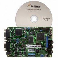
Manufacturer Part Number
DSP56309EVM
Description
KIT EVALUATION FOR XC56309
Manufacturer
Freescale Semiconductor
Type
DSPr
Specifications of DSP56309EVM
Contents
Module Board, Installation Guide, Power Supply, Cable, Software and more
Description/function
Audio DSPs
Product
Audio Modules
For Use With/related Products
DSP56309
Lead Free Status / RoHS Status
Contains lead / RoHS non-compliant


Programming Reference
B-24
Receive Exception Interrupt Enable
Application:
ESSI
0 = Disable
Transmit Exception Interrupt Enable
ESSI Control Register B (CRBx)
Reset = $000000
23 22 21 20
0 = Disable
REIE
Receive Last Slot Interrupt Enable
0 = Disable
Transmit Last Slot Interrupt Enable
0 = Disable
Receive Interrupt Enable
TEIE
0 = Disable
Transmit Interrupt Enable
0 = Disable
Receiver Enable
RLIE
0 = Disable
Transmit 0 Enable
0 = Disable
Transmit 1 Enable (SYN=1 only)
1 = Enable
0 = Disable
Transmit 2 Enable (SYN=1 only)
TLIE
1 = Enable
0 = Disable
Mode Select
1 = Enable
0 = Normal
Sync/Async Control
(Tx & Rx transfer together or not)
1 = Enable
19 18 17 16
RIE
1 = Synchronous
0 = Asynchronous
1 = Enable
1 = Enable
TIE
Figure B-15. ESSI Control Register B (CRB)
1 = Enable
1 = Enable
1 = Enable
RE
1 = Enable
1 = Network
TE0
15 14 13 12 11 10 9
DSP56309 User’s Manual, Rev. 1
TE1 TE2 MOD SYN CKP
ESSI0—X:$FFFFB6 Read/Write
ESSI1—X:$FFFFA6 Read/Write
Clock Polarity
(clk edge data & Frame Sync clocked out/in)
0 = out on rising/in on falling
1 = in on rising/out on falling
Frame Sync Polarity
FSP FSR FSL1
1 = low level (negative)
0 = high level (positive)
Frame Sync Relative Timing
(WL Frame Sync only)
1 = 1 clock cycle earlier than first data bit
0 = with first data bit
FSL1
0
0
1
1
Shift Direction
8
Clock Source Direction
0 = MSB First
0 = External Clock
FSL0
FSL0
7
0
1
0
1
SC0
SC1
SC2
Pin
Serial Control Direction Bits (see Table 8-2)
SHFD
Word
Bit
Bit
Word
6
Date:
Programmer:
Frame Sync
TX
Length
SCKD SCD2 SCD1 SCD0 OF1 OF0
Rx Clk
Rx Frame Sync
Tx Frame Sync
5
SCDx = 0 (Input)
Word
Word
Bit
Bit
1 = LSB First
RX
Output Flag x
4
If SYN = 1 and SCD1 = 1
OFx → SCx Pin
1 = Internal Clock
3
Freescale Semiconductor
2
Sheet 2 of 3
Flag 0
Flag 1
Tx, Rx Frame Sync
SCDx = 1 (Output)
1
0
Related parts for DSP56309EVM
Image
Part Number
Description
Manufacturer
Datasheet
Request
R

Part Number:
Description:
Manufacturer:
Freescale Semiconductor, Inc
Datasheet:
Part Number:
Description:
Manufacturer:
Freescale Semiconductor, Inc
Datasheet:
Part Number:
Description:
Manufacturer:
Freescale Semiconductor, Inc
Datasheet:
Part Number:
Description:
Manufacturer:
Freescale Semiconductor, Inc
Datasheet:
Part Number:
Description:
Manufacturer:
Freescale Semiconductor, Inc
Datasheet:
Part Number:
Description:
Manufacturer:
Freescale Semiconductor, Inc
Datasheet:
Part Number:
Description:
Manufacturer:
Freescale Semiconductor, Inc
Datasheet:
Part Number:
Description:
Manufacturer:
Freescale Semiconductor, Inc
Datasheet:
Part Number:
Description:
Manufacturer:
Freescale Semiconductor, Inc
Datasheet:
Part Number:
Description:
Manufacturer:
Freescale Semiconductor, Inc
Datasheet:
Part Number:
Description:
Manufacturer:
Freescale Semiconductor, Inc
Datasheet:
Part Number:
Description:
Manufacturer:
Freescale Semiconductor, Inc
Datasheet:
Part Number:
Description:
Manufacturer:
Freescale Semiconductor, Inc
Datasheet:
Part Number:
Description:
Manufacturer:
Freescale Semiconductor, Inc
Datasheet:
Part Number:
Description:
Manufacturer:
Freescale Semiconductor, Inc
Datasheet: