DSP56309EVM Freescale Semiconductor, DSP56309EVM Datasheet - Page 27
DSP56309EVM
Manufacturer Part Number
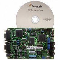
DSP56309EVM
Description
KIT EVALUATION FOR XC56309
Manufacturer
Freescale Semiconductor
Type
DSPr
Specifications of DSP56309EVM
Contents
Module Board, Installation Guide, Power Supply, Cable, Software and more
Description/function
Audio DSPs
Product
Audio Modules
For Use With/related Products
DSP56309
Lead Free Status / RoHS Status
Contains lead / RoHS non-compliant


2.1 Power
2.2 Ground
Freescale Semiconductor
V
V
V
V
V
V
V
Note:
GND
GND
GND
CCP
CCQ
CCA
CCD
CCC
CCH
CCS
Power Name
Ground Name
P
P1
Q
(4)
(2)
(4)
(4)
(2)
(4)
These designations are package-dependent. Some packages connect all V
internally. On those packages, all power input except V
in this table are minimum values; the total V
PLL Power
V
should be provided with an extremely low impedance path to the V
Quiet Power
An isolated power for the internal processing logic. This input must be tied externally to all other chip
power inputs, except for V
Address Bus Power
An isolated power for sections of the address bus I/O drivers. This input must be tied externally to all other
chip power inputs, except for V
Data Bus Power
An isolated power for sections of the data bus I/O drivers. This input must be tied externally to all other
chip power inputs, except for V
Bus Control Power
An isolated power for the bus control I/O drivers. This input must be tied externally to all other chip power
inputs, except for V
Host Power
An isolated power for the HI08 I/O drivers. This input must be tied externally to all other chip power inputs,
except for V
ESSI, SCI, and Timer Power
An isolated power for the ESSI, SCI, and timer I/O drivers. This input must be tied externally to all other
chip power inputs, except for V
PLL Ground
Ground dedicated for PLL use. The connection should be provided with an extremely low-impedance
path to ground. V
to the chip package.
PLL Ground 1
Ground dedicated for PLL use. The connection should be provided with an extremely low-impedance
path to ground.
Quiet Ground
An isolated ground for the internal processing logic. This connection must be tied externally to all other
chip ground connections, except GND
decoupling capacitors.
CC
dedicated for use with Phase Lock Loop (PLL). The voltage should be well-regulated and the input
CCP
. The user must provide adequate external decoupling capacitors.
CCP
CCP
should be bypassed to GND
. The user must provide adequate external decoupling capacitors.
DSP56309 User’s Manual, Rev. 1
Table 2-2. Power Inputs
CCP
Table 2-3. Grounds
. The user must provide adequate external decoupling capacitors.
CCP
CCP
CCP
CC
. The user must provide adequate external decoupling capacitors.
. The user must provide adequate external decoupling capacitors.
. The user must provide adequate external decoupling capacitors.
connections are package-dependent.
P
and GND
CCP
Description
Description
are labeled V
P1
P
. The user must provide adequate external
by a 0.47 µF capacitor located as close as possible
CC
CC
. The numbers of connections indicated
CC
inputs except V
power rail.
CCP
to each other
Power
2-3
Related parts for DSP56309EVM
Image
Part Number
Description
Manufacturer
Datasheet
Request
R

Part Number:
Description:
Manufacturer:
Freescale Semiconductor, Inc
Datasheet:
Part Number:
Description:
Manufacturer:
Freescale Semiconductor, Inc
Datasheet:
Part Number:
Description:
Manufacturer:
Freescale Semiconductor, Inc
Datasheet:
Part Number:
Description:
Manufacturer:
Freescale Semiconductor, Inc
Datasheet:
Part Number:
Description:
Manufacturer:
Freescale Semiconductor, Inc
Datasheet:
Part Number:
Description:
Manufacturer:
Freescale Semiconductor, Inc
Datasheet:
Part Number:
Description:
Manufacturer:
Freescale Semiconductor, Inc
Datasheet:
Part Number:
Description:
Manufacturer:
Freescale Semiconductor, Inc
Datasheet:
Part Number:
Description:
Manufacturer:
Freescale Semiconductor, Inc
Datasheet:
Part Number:
Description:
Manufacturer:
Freescale Semiconductor, Inc
Datasheet:
Part Number:
Description:
Manufacturer:
Freescale Semiconductor, Inc
Datasheet:
Part Number:
Description:
Manufacturer:
Freescale Semiconductor, Inc
Datasheet:
Part Number:
Description:
Manufacturer:
Freescale Semiconductor, Inc
Datasheet:
Part Number:
Description:
Manufacturer:
Freescale Semiconductor, Inc
Datasheet:
Part Number:
Description:
Manufacturer:
Freescale Semiconductor, Inc
Datasheet: